In complex PCB designs, there's a small but critical element that often goes unnoticed — jumpers. They act as "bridges" in the circuit, connecting components and solving layout challenges. But jumper usage is not arbitrary. Used correctly, they are an invaluable tool; used poorly, they can cause instability or functional failure.
This article provides a practical engineering overview of PCB jumpers — covering types, applications, common pitfalls, and design rules to help hardware engineers use jumpers effectively in their designs.
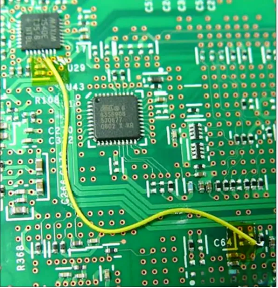
A jumper is a special connection used in PCB design to bridge "breaks" in the circuit. It typically takes the form of thicker wires, resistors, solder bridges, or specific PCB traces, solving problems such as:
Components that cannot be directly connected: When layout space is limited and component pins cannot be routed directly, jumpers provide an alternative path
Components placed too far apart: On large PCBs, certain signals need to cross long distances; jumpers can shorten critical paths
Pin assignment errors needing correction: When schematic or footprint definitions have errors, jumpers can serve as an engineering fix
Limited routing resources on single-sided or double-sided boards: In cost-sensitive low-layer-count designs, jumpers add routing flexibility without increasing layer count
Different jumper types suit different design scenarios. Understanding their respective advantages and disadvantages is key to making the right choice:
Characteristics: Insulated wires soldered directly to PCB pads — the most traditional and direct jumper method.
Best For: Prototype verification, small-scale engineering fixes, cross-connections on single-sided or double-sided boards.
Advantages: Simple to implement, low cost, easy to modify.
Disadvantages: Requires manual soldering in production, increasing assembly cost; excessively long or bent wires may cause signal integrity issues.
Characteristics: Use 0Ω resistors or specific value SMD resistors as jumper elements.
Best For: Production designs requiring configurable options (e.g., enabling different functional modules).
Advantages: Compatible with SMT automated production processes; eliminates additional manual soldering steps; values can be changed for fine-tuning.
Disadvantages: Occupies PCB surface space; 0Ω resistors still have minor parasitic effects at high frequencies.
Characteristics: Bridging adjacent pads on the PCB with a solder connection.
Best For: Configuration switching, on-site adjustments during production.
Advantages: No additional component space; can be decided during test or configuration.
Disadvantages: Requires skilled soldering; bridge quality is hard to control consistently; difficult to rework.
Characteristics: Jumper function implemented through PCB connection holes or special traces.
Best For: Production designs requiring configurable jumper options.
Advantages: Integrated into the PCB manufacturing process; no extra material cost; high reliability.
Disadvantages: Design changes require a board revision.
The most basic function of jumpers is to resolve "deadlocks" in routing — when signals cannot be completed within the available layers, jumpers provide an additional routing channel, allowing the design to proceed.
In high-power or mixed-signal circuits, jumpers can separate different functional regions, preventing noise from coupling through common paths into sensitive circuits.
During prototyping and production, jumpers serve as configuration options or debugging tools, making designs more flexible and easier to modify or extend later.
While jumpers are useful, falling into these traps can compromise the entire design:
Long jumpers act as "antennas," picking up or radiating noise, leading to signal attenuation or EMI issues.
Correct Practice: Keep jumper routing as short as possible; avoid "U" or "S" curves in the path.
Jumpers placed near sensitive circuits (high-speed signal paths, analog front-ends, RF regions) can introduce coupling interference.
Correct Practice: Position jumpers away from critical signal areas; prioritize low-risk routing zones.
Hand-soldered jumpers with poor quality connections can cause intermittent faults that are difficult to diagnose.
Correct Practice: Prefer resistor or PCB jumpers for production designs. If wire jumpers must be used, define clear soldering process specifications and inspect solder joints.
Jumpers without proper return path treatment can create ground loop issues, causing EMI or noise coupling.
Correct Practice: Maintain a continuous ground plane around jumpers to ensure complete signal return paths.
Keep jumper paths as short and direct as possible. Shorter length means less signal attenuation and better noise immunity. Avoid unnecessary coils or detours. This principle applies to all jumper types — wire, solder, or PCB jumpers — keep the routed length to a minimum.
Keep jumpers away from high-frequency signals, analog signals, clocks, and RF traces. Maintain safe clearance. For wire jumpers especially, avoid long parallel runs with sensitive signals.
When using wire jumpers, inspect solder joints with a magnifying glass or microscope to ensure no cold or insufficient joints.
Before powering on, use a multimeter to check jumper continuity and resistance values.
Wire jumpers require manual intervention in production, potentially reducing efficiency and increasing labor costs. For high-volume production, prioritize automation-compatible solutions like 0Ω resistor jumpers or PCB jumpers.
Jumpers are a common technique in PCB design, but incorrect usage can be counterproductive. For hardware engineers, understanding the characteristics, applications, and design constraints of different jumper types is essential for making informed decisions in real projects.
In single-sided or double-sided boards where space is limited, or during prototyping, jumpers effectively solve routing problems. In production designs, however, the trade-offs between jumpers and their impact on cost and reliability should be carefully weighed, with priority given to automated production solutions.
Need PCB Design Support?
AnyPCBA's engineering team focuses on jumper placement, signal integrity, and manufacturability during design reviews. Whether you're working on prototype verification or production preparation, we provide DFM/DFA design reviews to identify potential risks in jumper routing, layout, and stackup before fabrication.
Our manufacturing capabilities cover 2-64 layers, including HDI, rigid-flex, and high-frequency hybrid processes.
Contact us to discuss your project →