In PCB design and manufacturing, one file format plays a critical bridging role: the Gerber file. It is the key data carrier connecting design engineers and manufacturing facilities, carrying all the information needed to transform a circuit design into a physical circuit board.
This article provides a comprehensive introduction to Gerber files — covering their basic concepts, structure, formats, generation methods, and applications in PCB manufacturing — to help hardware engineers better understand and use this essential tool.
A Gerber file is a standard format used in electronic design automation (EDA), particularly in PCB design and manufacturing, to convey circuit layer information, pads, traces, component placement, and more. It serves as the critical bridge from the design phase to the production phase, providing manufacturers with precise production information.
Simply put, a Gerber file is the "digital language" of PCB design drawings, enabling manufacturers to accurately interpret the designer's intent and produce accordingly.
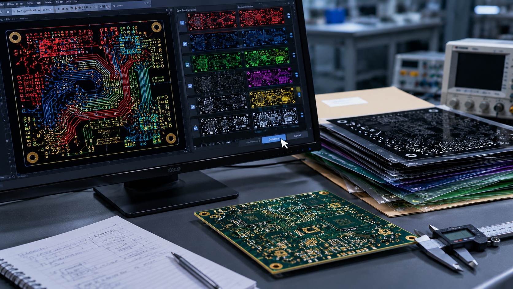
A Gerber file typically consists of multiple files, each describing a specific layer of the PCB. The typical Gerber file composition includes:
| File Type | Description | Importance |
|---|---|---|
| Copper Layers | Describes the electrical connections — signal layers, power layers, ground layers, etc. | Core files determining circuit functionality |
| Solder Mask Layer | Defines areas covered by solder mask and areas exposed for soldering | Affects soldering quality and reliability |
| Silkscreen Layer | Displays component designators, outlines, polarity markers, and text | Aids manual assembly and debugging |
| Drill Layer | Indicates hole locations — component pins, vias, test points, etc. | Determines drilling accuracy |
| Outline Layer | Defines the PCB's outer shape and routing slots | Determines the final board shape |
These layers together form the complete PCB manufacturing data package — none can be omitted.
Gerber files use a vector graphic format, with each file containing path descriptions of PCB layers. There are two main Gerber formats:
| Format | Characteristics | Usage Status |
|---|---|---|
| RS-274X | Extended format with complete graphic information; no separate auxiliary files needed | Currently the most widely used standard |
| RS-274-D | Older format requiring separate auxiliary files for graphic information | Largely obsolete; limited to legacy equipment |
RS-274X has become the industry standard, supported by most modern EDA tools and PCB manufacturers.
Gerber files are typically generated through EDA software such as Altium Designer, Eagle, KiCad, Cadence Allegro, and others. The generation process requires attention to several key aspects:
Ensure every design layer (signal layers, power layers, silkscreen, solder mask, etc.) is correctly output — nothing should be missed.
Gerber files define path precision, typically at the micron level, ensuring all board details are accurately conveyed to the manufacturer.
All hole locations on the PCB need to be precisely described through the drill layer.
Ensure all aperture definitions for trace widths and pad sizes are correctly included in the files.
Gerber files are the most fundamental and important data format in PCB manufacturing, used across multiple stages:
PCB Fabrication
Manufacturers use copper layer and solder mask information for photolithography, etching, and plating processes.
Component Placement and Soldering
Silkscreen and component placement layers guide precise component positioning and soldering areas for SMT assembly.
Drilling
The drill layer provides accurate hole location and size information for drilling machines.
Electrical Testing
Copper layer information can also generate netlist data for flying probe or ICT testing to verify electrical connectivity.
Once Gerber files are generated, they are sent to the PCB manufacturer. To ensure manufacturing accuracy, the following validation steps are recommended:
Designers should use a Gerber Viewer to inspect files and confirm each layer matches expectations. These tools simulate layer stacking to help identify potential design errors.
At AnyPCBA, we recommend using DFM (Design for Manufacturability) tools to review Gerber files, ensuring they meet manufacturing process requirements and identifying potential yield issues early.
Before production, confirm file formats, precision requirements, and special instructions with the manufacturer's engineering team to avoid misunderstandings.
Gerber files contain complex graphic paths and multiple layers. Any minor error can cause manufacturing defects. Ensuring file accuracy and completeness is essential.
Solution: Use Gerber validation tools for systematic checks and establish standardized file output procedures.
Different Gerber file versions may have format differences. Compatibility must be ensured when transferring across platforms.
Solution: Standardize on RS-274X format and avoid using older formats.
As design complexity increases (multilayer PCBs, HDI, rigid-flex, etc.), Gerber file management becomes more challenging.
Solution: Establish clear layer naming conventions and regularly check file completeness.
Gerber files are an essential format in PCB design and manufacturing, used to precisely describe patterns for each PCB layer. They provide PCB manufacturers with detailed design requirements, ensuring smooth transition from design to production.
Through accurate generation, transfer, and validation of Gerber files, design errors can be significantly reduced, manufacturing efficiency improved, and product quality enhanced. In modern electronics manufacturing, Gerber files remain one of the most widely used standard data formats.
Need Gerber File Review or PCB Manufacturing Support?
AnyPCBA's engineering team provides Gerber file DFM review services, helping you identify potential design issues before production and optimize manufacturing processes. Our manufacturing capabilities cover 2-64 layers, including HDI, rigid-flex, and high-frequency hybrid processes.
Contact us to discuss your project →