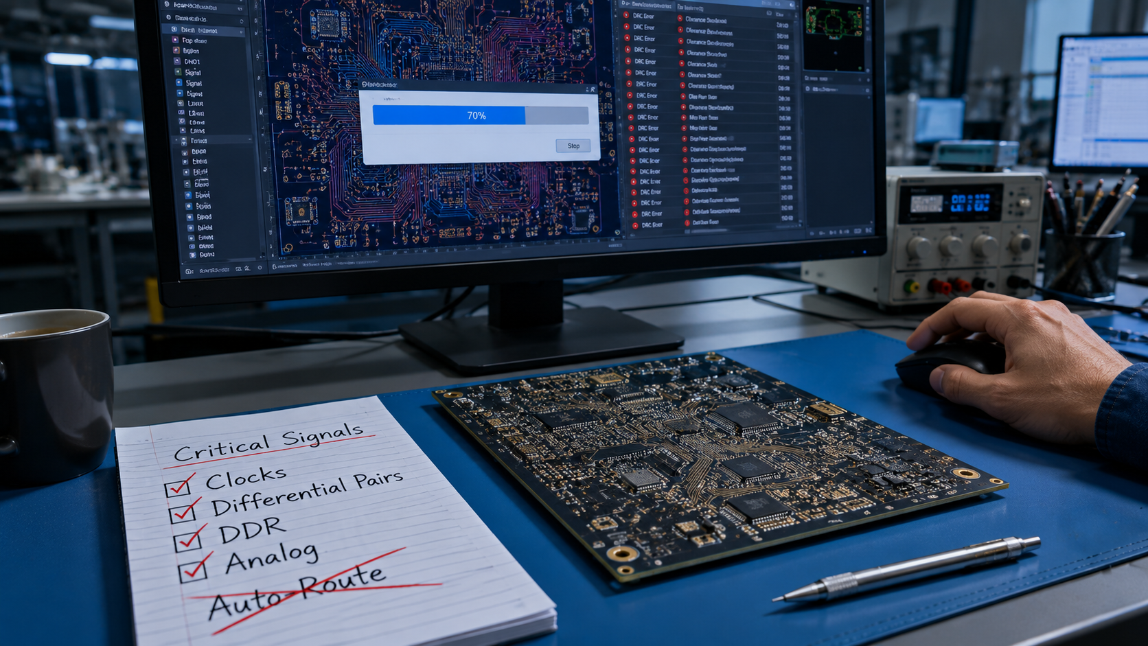
Every time a new engineer reaches for the auto-route button, someone with experience winces. It's not that auto-routing is useless — for slow, low-complexity boards, it saves time and ensures basic connectivity. But when your design is fast and complex, auto-routing is a time bomb waiting to explode.
Many hardware engineers learn this the hard way: schematic is correct, components are properly selected, layout and routing are fully automated. The prototype comes back — and nothing works. Bit error rates are through the roof. EMI tests fail. The root cause? Almost always, routing hidden issues.
This article explains why high-speed PCBs can't be fully auto-routed and where the baseline for manual routing really is.
Many junior designers think PCB routing is just connecting the dots. They've never worked on a 10Gbps+ project.
Low-speed signals are essentially digital 0s and 1s traveling slowly. Some interference, some reflections — not a big deal. The receiver has enough margin to handle them.
High-speed signals are a completely different animal. They travel as electromagnetic waves on transmission lines. At high frequencies, signal integrity issues emerge.
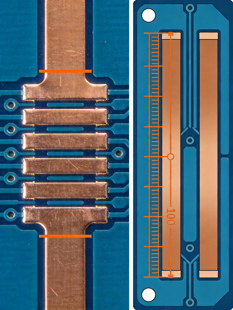
A 5GHz signal has a wavelength of about 3 centimeters. When your trace length approaches this scale, the trace stops being a simple wire — it becomes an antenna, a transmission line. Impedance must be tightly controlled; otherwise, signals reflect back and cause overshoot, undershoot, and ringing.
Industry standard: single-ended impedance at 50Ω, differential at 100Ω. Even 10% deviation can break a high-speed design. This precision requirement is far beyond what auto-routing's "close enough" logic can handle.
An auto-router is essentially a "maze-solving tool." Its core logic is: find a path from point A to point B while meeting your spacing and width rules. It doesn't care if the signal runs at 5Mbps or 5Gbps. It doesn't care if it's a clock or a regular I/O. And it certainly doesn't care if the return path is ten miles long.
In high-speed scenarios, this creates a chain of problems.
High-speed signals require continuous, precise impedance matching. Impedance is determined by four factors: trace width, copper thickness, dielectric thickness, and dielectric constant. The auto-router blindly follows your preset trace width, but at corners, vias, and layer transitions, impedance has already drifted to unknown values.
One PCIe Gen3 board routed with auto-router had impedance errors exceeding 20% — borderline unusable.
USB, HDMI, PCIe, Ethernet — these high-speed interfaces rely on differential pairs. The principle is simple: two traces carry opposite signals, and the receiver subtracts them to cancel noise. But the trade-off is strict: these two traces must be equal in length, equal in spacing, and symmetrical. Length mismatch must stay within 5 mils. Spacing must be constant.
Can auto-routing do this? Not a chance. It will either create a long-short mismatch or let the two traces wander with inconsistent spacing. The consequences: timing skew, common-mode noise, and eye diagram closure — every one of them a death sentence for high-speed designs.
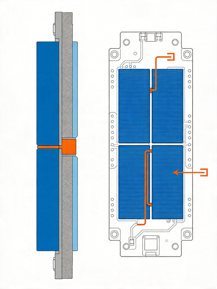
High-speed PCBs have dense routing. Adjacent traces couple through electromagnetic fields, creating crosstalk. The 3W rule (spacing ≥ 3× trace width) is there for a reason. Auto-routing prioritizes completion rate. It doesn't care if two high-speed traces are tightly coupled for 10mm. The board comes back, near-end and far-end crosstalk both exceed limits, and debugging is a nightmare.
This is the most overlooked but most fatal issue. High-speed signals are not one-way tickets; they require return currents. The shorter the return path and the smaller the loop area, the better. Ideally, there's a solid ground plane directly under the trace, and the return current follows closely — loop area close to zero.
Auto-routing loves to cross plane splits, detour around vias, and change layers — every step disrupts the return path. The result: loop area multiplies, and EMI radiation goes through the roof.
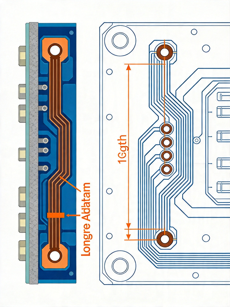
With all these auto-routing issues, does manual routing guarantee success? Not necessarily. The key is knowing which signals must be routed manually and which can be trusted to software.
Based on experience, these signals require manual routing:
Crystals, clock generators, PLLs — these are the board's heartbeat. Clock lines must be short, straight, with complete return paths, and kept away from noise sources. Auto-routing will happily send them on a scenic tour.
USB, HDMI, PCIe, SATA, MIPI, Ethernet — every differential signal needs manual attention. Width, spacing, length matching — no compromise on any parameter.
Length matching requirements are extremely strict — data groups, address groups, control groups, each with tight length tolerances, typically within ±5 mils.
Though not "high-speed," high-current paths need careful planning: wide copper, plenty of vias, minimal loop area — otherwise, excessive voltage drop and heat generation.
ADC front-ends, sensor signals, RF traces — these directly affect the noise floor. Auto-routed traces will quickly destroy the signal-to-noise ratio.
The most effective workflow is hybrid routing: manually route critical, high-precision signals and lock them, then let auto-routing handle the rest.
Recommended workflow:
Define stackup and impedance targets based on schematic and datasheets
Manually route all critical signals (clocks, differential pairs, DDR, etc.)
Set up rule constraints and let auto-routing handle power, ground, and low-speed signals
Perform full review and manual fine-tuning
This approach ensures high-speed signal quality while maintaining design efficiency. The key is engineering judgment — knowing what to route manually and what to leave to software.
Myth 1: Setting rules means everything is fine. Rules tell the software "how you should route," not that it will route correctly. The result must be checked.
Myth 2: Simulation is enough. Simulation models are mathematical approximations — there's always a gap between models and real boards. Passing simulation only means "probably fine," not "definitely fine."
Myth 3: We can fix it in the lab. The reality is, routing issues in high-speed PCBs are extremely difficult to fix after the board is manufactured. Impedance mismatch, crosstalk, EMI — if not addressed at the design stage, they mean a respin.
Low-speed designs are about connectivity. High-speed designs are about impedance.
Auto-routing is a useful tool for simple boards. For high-speed digital PCBs, it can only serve as a support — the real design quality comes from engineering experience and judgment.
Getting connectivity right makes you a competent engineer. Getting high-speed signals right makes you a senior engineer.
Need Support for High-Speed PCB Design?
AnyPCBA's engineering team focuses on impedance control, differential pair routing, crosstalk suppression, and return path integrity during design reviews. Whether you're using auto-routing assistance or full manual routing, we provide DFM design reviews to identify potential high-speed signal integrity issues before fabrication.
Our manufacturing capabilities cover 2-64 layers, including HDI, rigid-flex, and high-frequency hybrid processes.
Contact us to discuss your project →