
In the fast-evolving landscape of smart security, integrating biometric sensors into compact, power-constrained PCBAs presents significant engineering hurdles. A minor oversight in Design for Manufacturing (DFM) can lead to costly delays and product recalls. This guide bridges the gap between sophisticated sensor requirements and efficient, high-yield manufacturing processes.
Understanding the Unique Constraints of Biometric Sensors
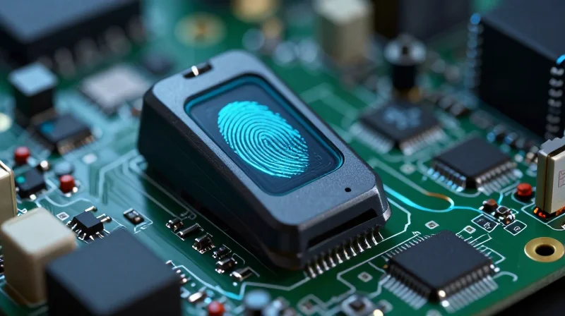
Navigating Signal Integrity in Biometric Assemblies
Biometric sensors, particularly capacitive fingerprint scanners and sub-dermal vein recognition modules, function by measuring infinitesimal electrical fluctuations. In a high-density smart lock PCBA, these sensors operate in extreme proximity to switching regulators, radio frequency (RF) antennas, and mechanical actuators. Maintaining signal integrity requires rigorous adherence to electromagnetic compatibility (EMC) standards to prevent noise from masking the biometric signal, which could lead to false rejection rates (FRR) or complete authentication failure.
Key Environmental and Interference Challenges
| Challenge Factor | Biometric Impact | DFM Mitigation Strategy |
|---|---|---|
| Thermal Variance | Sensor baseline drift | Isolate heat-generating components |
| Electromagnetic Noise | Signal-to-noise ratio degradation | Differential signaling and guard traces |
| Mechanical Vibration | False contact detection | Dampened mounting and rigid-flex zones |
Frequently Asked Questions
- How does thermal variance affect biometric accuracy?
Biometric sensors rely on precise capacitance or infrared reflectance measurements; temperature fluctuations can shift the electrical baseline of the sensor, requiring real-time calibration algorithms to avoid degraded performance. - What is the primary risk of high-density component placement near scanners?
The proximity of switching power supplies or high-speed data lines introduces EMI, which can capacitively couple into the sensitive input stages of the sensor, causing significant noise artifacts in the raw capture data. - Why is grounding strategy critical for vein scanners?
Vein scanners utilize low-level infrared reflection; inconsistent ground planes create ground loops that induce image noise, necessitating a 'star' grounding approach or a dedicated clean analog ground plane isolated from the main processor digital ground.
Strategic Component Placement for Signal Integrity
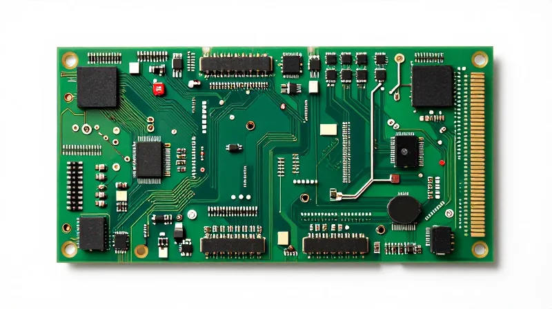
Minimizing Trace Lengths for Sensitive Biometric Signals
In smart security locks, the analog output from biometric sensors is inherently susceptible to signal degradation. To maintain high-fidelity data capture, place the Analog Front End (AFE) as close as possible to the sensor interface. Shortening the physical trace length minimizes the parasitic capacitance and inductance that can distort raw biometric images, effectively lowering the noise floor and preventing bit-error rate spikes during authentication.
Strategies for Digital-Analog Isolation
High-density PCBAs suffer from electromagnetic interference (EMI) generated by high-speed digital switching circuits. Implementing a robust isolation strategy is critical to protect sensitive sensor data paths.
| Strategy | Implementation | Benefit |
|---|---|---|
| Ground Plane Splitting | Use separate AGND/DGND planes linked at a single point | Prevents digital return currents from injecting noise into the sensor ground |
| Trace Routing | Route analog signals perpendicular to high-speed digital lines | Minimizes inductive coupling and cross-talk |
| Shielding | Apply a grounded guard trace around analog signal routes | Provides a stable reference and blocks capacitive interference |
Common Implementation Questions
- How does layer stack-up impact signal integrity in thin smart locks?
A well-designed stack-up utilizes internal solid ground planes between signal layers. This configuration provides a continuous return path and significantly reduces the loop area for high-speed signals. - Is via placement critical for biometric sensors?
Yes. Avoid vias on sensitive analog traces. If routing between layers is mandatory, ensure a via is placed near the signal path to connect the ground planes, preventing impedance discontinuities. - How should I handle power distribution for noise-sensitive components?
Use dedicated ferrites and low-ESR decoupling capacitors localized directly at the sensor power pins to filter out high-frequency transients originating from the MCU or wireless communication modules.
Optimizing Trace Width and Via Spacing in HDI Designs

Precision Routing for Signal Integrity
In smart security locks, where biometric modules share board space with high-speed processors, HDI (High-Density Interconnect) routing is critical. Maintaining impedance control requires tight tolerances on trace widths. As signals transition through layers via micro-vias, parasitic capacitance and inductance must be minimized to prevent signal degradation and crosstalk that could trigger false biometric readings.
| Feature | Standard HDI Recommendation | High-Speed Requirement |
|---|---|---|
| Trace Width | 3-4 mil | 2.5-3 mil (Controlled Impedance) |
| Via-to-Trace Clearance | 4 mil | 5-6 mil (Reduce Coupling) |
| Via-to-Via Pitch | 10-12 mil | 15+ mil (Staggered Pattern) |
Key HDI Design Considerations for Biometric Modules
- How do I mitigate crosstalk between biometric analog lines and high-speed digital clocks?
Increase the physical spacing between the analog sensor traces and digital lines by at least 3x the dielectric height. Utilize grounded guard traces or shield layers for sensitive analog signal paths. - Why is micro-via structure important for impedance stability?
Micro-vias provide shorter electrical paths compared to through-hole vias. Using blind or buried vias reduces the parasitic stub effect, which is vital for maintaining consistent characteristic impedance at high frequencies. - What is the recommended trace width tolerance for biometric sensors?
For sensitive analog paths, specify a strict ±10% width tolerance. Variations in width significantly alter trace impedance, which can lead to signal reflections that introduce noise into the fingerprint capture process.
Best Practices for Via Stacking
While stacked vias save space, they can create thermal stress points. In biometric modules exposed to temperature fluctuations, favor staggered via designs to improve reliability. If stacking is necessary, ensure copper filling is specified in the manufacturing notes to prevent voids that compromise signal integrity and thermal dissipation.
Surface Mount Technology (SMT) Considerations for Miniaturization
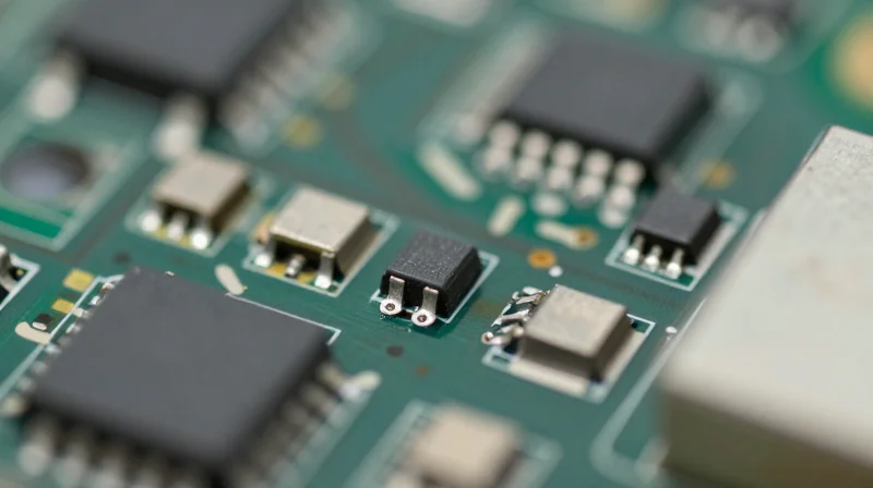
SMT Packaging and Miniaturization Constraints
As smart security locks shrink, moving to 0201 or 01005 metric packages becomes necessary but complicates manufacturing tolerances. For biometric PCBA, selecting the correct package isn't just about size; it's about balancing thermal dissipation requirements for fingerprint sensors with the structural integrity needed to withstand the mechanical vibrations of deadbolt engagement. Designers must prioritize packages with larger terminal areas to enhance solder joint reliability in high-g conditions.
Land Pattern Optimization for HDI
Standard IPC-7351 land patterns often require scaling to accommodate HDI fabrication tolerances. When routing traces between pads, consider non-solder mask defined (NSMD) pads to improve registration and solder wetting. For biometric sensing components, strict adherence to the manufacturer's suggested stencil aperture size is vital; excessive solder paste can create 'tombstoning' on small passive components or cause bridges that compromise sensitive analog signal integrity.
| Package Type | Miniaturization Benefit | DFM Risk Factor | Recommendation |
|---|---|---|---|
| 0201 / 0603 | High density | Solder bridging | Use laser-cut stencils |
| BGA / WLCSP | Vertical integration | Underfill stress | Strict reflow profiling |
| QFN | Thermal performance | Thermal pad voids | Window-pane aperture |
Technical FAQ: SMT Best Practices
- How do we prevent tombstoning in high-density zones?
Ensure balanced copper distribution around component pads and utilize smaller stencil apertures to minimize excessive paste volume which contributes to uneven thermal wetting forces. - Is underfill mandatory for biometric sensors?
If the lock assembly is subject to high mechanical impact or frequent vibration, underfilling BGA/WLCSP sensors is highly recommended to protect solder balls from shear fatigue. - What is the impact of via-in-pad on SMT yield?
Via-in-pad technologies are essential for space-saving, but they must be capped, plated, and flattened to avoid 'solder starvation,' where paste wicks into the barrel during reflow.
Thermal Management in Compact Smart Lock Enclosures

Managing Thermal Density in Confined Enclosures
In the confined architecture of a smart lock, the proximity of the main application processor to the biometric sensor array creates a significant thermal challenge. Excessive heat buildup not only degrades the accuracy of fingerprint scanning hardware but can also lead to long-term reliability issues for the PCBA. Implementing robust thermal dissipation strategies—such as integrating thermal vias, utilizing high-conductivity interface materials, and establishing clear conductive paths to the external chassis—is essential to maintaining operating temperatures within safe limits.
Thermal Mitigation Strategies
| Strategy | Primary Function | DFM Impact |
|---|---|---|
| Thermal Vias | Conduct heat to internal copper planes | Requires strict drill spacing to avoid board weakening |
| TIM Application | Bridge gaps between SoC and chassis | Must account for compression and assembly tolerance |
| Component Standoffs | Increase surface area for convection | Limited by Z-height constraints in smart locks |
Frequently Asked Questions
- How does heat impact biometric sensor accuracy?
Capacitive and optical sensors are sensitive to thermal drift. Excessive heat can alter the dielectric properties or light refraction levels, leading to increased false rejection rates (FRR) or sensor noise. - Why is the enclosure chassis important for thermal relief?
Since smart locks lack active cooling like fans, the metal housing serves as the primary heat sink. Designing the PCBA to interface directly with the chassis via thermal pads or heat spreaders effectively increases the mass available for heat dissipation. - What is the primary constraint when adding thermal vias?
The main constraint is balancing thermal performance against signal integrity. Dense vias can create impedance discontinuities in high-speed digital traces if not properly mapped to return paths.
Minimizing Manufacturing Defects through Design Rule Checks
Automated DRC for Pre-Production Defect Prevention
Design Rule Checks (DRC) serve as the final gatekeeper in the DFM process for high-density smart lock electronics. By automating these checks within the CAD environment, engineers can identify geometric violations—such as insufficient annular rings or sliver-prone solder masks—before a single physical board is fabricated, effectively eliminating the cost of iterative prototype revisions.
Critical DFM Parameters for Biometric Assemblies
| Design Constraint | Common Failure Risk | DRC Correction Strategy |
|---|---|---|
| Stencil Aperture | Solder bridging or insufficient volume | Scale apertures based on pitch and component profile |
| Solder Mask Clearance | Copper oxidation or solder shorts | Enforce minimum 0.1mm web between pads |
| Panelization Edge | Board warping or router stress | Maintain 10mm buffer from PCB edges to sensitive traces |
Frequently Asked Questions
- How does DRC help prevent stencil design issues?
Automated DRC confirms that aperture-to-pad ratios align with your specific solder paste chemistry, preventing the excess paste that causes shorts in tight biometric sensor arrays. - What is the role of DRC in panelization efficiency?
DRC ensures that break-away tabs and fiducial markings are positioned correctly to maximize panel utilization while preventing mechanical damage to the PCBA during de-paneling. - Why is solder mask clearance critical for biometric devices?
In high-density locks, tight clearances risk solder mask encroachment, which leads to weak joints on small-pitch connectors and potential failure of the biometric feedback signal.
Collaborating with Contract Manufacturers for Success
Strategic Alignment for NPI Success
The transition from prototype to mass production for high-density biometric security locks hinges on early-stage collaboration. Engaging your contract manufacturer (CM) during the schematic and layout phase prevents costly re-spins by ensuring your DFM rules align perfectly with the CM's specific equipment capabilities and process tolerances.
Communication Matrix
| Development Phase | Key Deliverable | Primary Goal |
|---|---|---|
| Conceptual | Board Architecture | Review stack-up and critical signal routing |
| Pre-Layout | DFM Guidelines | Verify assembly tolerances and component pitch |
| Proto-Release | Gerber/ODB++ Files | Ensure manufacturability and test point coverage |
Frequently Asked Questions
- Why should I share my DFM rules with the CM early?
Sharing rules early allows the CM to identify constraints, such as trace-to-hole ratios or pad clearances, that might fall outside their standard equipment capabilities, avoiding production delays later. - How does biometric sensor integration affect PCBA manufacturing?
Biometric modules often require specific thermal profiles and sensitive mounting tolerances; proactive discussion ensures the assembly process does not compromise sensor accuracy or integrity. - What role does the 'DFM Report' play in the NPI process?
The DFM report acts as a formal bridge between design intent and physical production, documenting agreed-upon modifications to ensure the board yield remains high during the first production run.
Technical Integration Checklist
To ensure long-term manufacturing consistency, establish a documented process for design handoffs. Focus on these three pillars: (1) Standardize file naming and version control, (2) Define clear solder mask and silkscreen tolerance limits, and (3) mutually agree on inspection standards (IPC-A-610 Class 2 or 3) prior to the first build.
By rigorously applying these DFM rules, you can transform your biometric sensor designs from fragile prototypes into rugged, mass-producible security solutions. Don't let manufacturing bottlenecks hold your innovation back. Contact our engineering team today for a comprehensive DFM audit of your next project.
