
In the demanding world of motor drive engineering, the margin for error is razor-thin. As currents climb and thermal constraints tighten, the integrity of your PCB becomes the single greatest bottleneck in your system's performance. Selecting the right copper weight isn't just about size; it's about engineering a foundation that handles power density without compromising board longevity.
Understanding Current-Carrying Capacity (Ampacity)

The Physics of Ampacity in Power Electronics
Ampacity, or current-carrying capacity, is the maximum current a conductor can handle before exceeding its rated temperature limit. In motor drive applications, high currents induce ohmic heating (I²R losses). Because the copper trace acts as a resistor, the goal is to balance trace cross-sectional area—defined by width and weight—against the allowable temperature rise of the PCB substrate.
Applying IPC-2152 Standards
The industry-standard IPC-2152 provides the mathematical framework for calculating trace heating. Unlike the older IPC-2221, which relied on overly conservative static curves, IPC-2152 utilizes a physics-based approach that accounts for thermal conductivity, dielectric material properties, and surrounding environments. Proper sizing requires engineers to specify a maximum allowable temperature rise (typically 10°C to 20°C above ambient) to ensure the longevity of both the PCB and the mounted power components.
| Parameter | Effect on Ampacity | Design Consideration |
|---|---|---|
| Copper Weight | Higher weight increases cross-section, reducing resistance. | Standardize on 2oz or 3oz copper for motor drives. |
| Trace Width | Wider traces lower resistance and increase surface area for cooling. | Space-constrained boards require internal layers for wider paths. |
| Temp Rise | Higher allowed temp rise permits smaller copper cross-sections. | Must balance against thermal limits of MOSFETs and ICs. |
Frequently Asked Questions
- Why is 1oz copper often insufficient for motor drives?
1oz copper (35µm) has high electrical resistance. In high-current applications, this leads to excessive voltage drops and heat buildup that can delaminate the board or exceed the thermal limits of surrounding semiconductors. - Does trace length impact ampacity?
While ampacity is defined by current density per unit of area, trace length increases total loop resistance. Longer traces create higher voltage drops and contribute more total heat to the system, necessitating wider copper paths. - How do internal layers contribute to cooling?
Internal layers are generally warmer due to poor convection. They require 50% to 100% more width compared to surface traces to achieve the same current capacity because they cannot dissipate heat into the air as effectively as top or bottom layers.
Thermal Management Challenges in High-Power Drives
The Dual Role of Heavy Copper as a Thermal Conductor
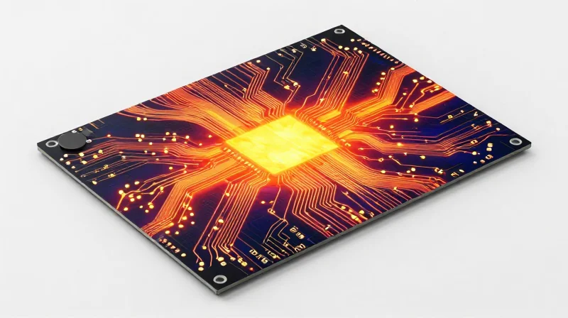
In high-current motor drive applications, thick copper PCBs function beyond mere electrical pathways; they serve as primary heat spreaders. Because copper possesses significantly higher thermal conductivity than the surrounding dielectric material, high-copper-weight layers effectively pull heat away from active switching components, such as MOSFETs and IGBTs. By increasing the cross-sectional area, the PCB trace effectively lowers the thermal resistance of the path, preventing local hot spots that could cause premature component failure or delamination of the board stackup.
Thermal Conductivity Interfaces
The efficacy of copper-based thermal management is intrinsically linked to the substrate material. While thick copper spreads heat laterally across the board surface, the vertical dissipation—moving heat from the top layer to an internal ground plane or the bottom of the PCB—is dictated by the thermal conductivity (k) of the prepreg and core materials. Engineers must pair heavy copper with high-Tg, thermally conductive dielectrics to ensure that the heat collected by the traces is efficiently transferred out of the PCB structure to the chassis or heat sink.
| Thermal Management Strategy | Primary Mechanism | Performance Impact |
|---|---|---|
| Lateral Spreading | Copper Trace Cross-section | Reduces localized component temperature spikes. |
| Vertical Transfer | Thermal Vias + Substrate K | Moves heat to heat-sink/chassis interface. |
| Heat Dissipation | Increased Surface Area | Improves convective cooling efficiency. |
Common Thermal Management FAQs
- Does doubling the copper weight halve the thermal resistance?
While increasing copper thickness significantly reduces electrical resistance and improves thermal mass, thermal resistance improvements are non-linear due to the influence of the substrate's interface resistance and the cooling environment. - Why is substrate thermal conductivity critical for high-power drives?
Standard FR-4 has poor thermal conductivity. High-power applications require specialized thermally conductive laminates to bridge the thermal gap between heavy copper traces and the secondary cooling system, preventing thermal bottlenecks. - How do thermal vias assist in thick copper designs?
Thermal vias act as vertical heat pipes. In heavy copper designs, they connect surface traces to internal planes, allowing the entire copper stackup to act as a unified heat sink.
Evaluating 3oz vs 6oz Copper: When to Upsize
Evaluating 3oz vs 6oz Copper: When to Upsize
The choice between 3oz and 6oz copper is rarely dictated by continuous current alone; it is primarily driven by transient peak load management and the board's thermal impedance. While 3oz copper often suffices for standard industrial motor drives, 6oz copper becomes mandatory when localized temperature rises threaten substrate integrity or when the trace width required for 3oz would consume excessive board real estate.
| Feature | 3oz Copper (105µm) | 6oz Copper (210µm) |
|---|---|---|
| Primary Application | General Industrial Drives | High-Torque/High-Inertia Drives |
| Thermal Capacity | Moderate Heat Spreading | High Thermal Mass/Sink |
| Space Efficiency | Standard footprint | High density (narrower traces) |
| Manufacturing Cost | Standard Heavy Copper | Premium/Advanced Fabrication |
Decision Criteria for Selecting 6oz Copper
- Peak Load Management
If the motor drive faces frequent, high-current startup stalls or dynamic braking events that exceed 3oz thermal limits for short durations, 6oz copper provides the necessary thermal mass to absorb these transients without exceeding glass transition temperature (Tg) limits. - Board Real Estate
When design constraints prohibit wide traces due to connector spacing or component density, 6oz copper allows you to maintain the required ampacity in a smaller physical width, effectively reducing the trace footprint by approximately 40-50% compared to 3oz. - System Reliability
In high-vibration or high-thermal-cycle environments, the mechanical stiffness of 6oz copper helps mitigate potential fatigue at solder joints and component interfaces, providing a more robust structural platform.
Engineering teams should perform a thermal simulation comparing 3oz and 6oz variants under the worst-case RMS current combined with worst-case ambient temperatures. If the simulation indicates the 3oz trace temperature approaches within 20°C of the substrate's maximum operating temperature, upgrading to 6oz is a strategic necessity to ensure long-term field reliability.
Power Integrity and Voltage Drop Mitigation
Minimizing Ohmic Losses for Motor Efficiency
In high-current motor drive applications, every milliohm of resistance contributes to ohmic losses (I²R), manifesting as both heat and voltage drop. By utilizing ultra-thick copper layers—typically 3oz to 6oz or greater—engineers can drastically reduce the DC resistance of power planes and traces. This reduction is critical not only for maintaining thermal stability but also for ensuring that the full intended voltage reaches the power stages of the motor driver, preventing motor torque degradation under peak load conditions.
Mitigation Strategies for High-Frequency Switching
High-frequency PWM switching introduces additional challenges, specifically regarding skin effect and EMI. Thick copper provides a larger cross-sectional area that mitigates these effects, while concurrently allowing for a lower inductance design. Properly placed return planes directly beneath high-current traces effectively cancel magnetic fields and minimize loop area, which is essential for signal stability and reducing switching noise in sensitive gate-drive circuits.
| Parameter | Standard Copper (1oz) | Thick Copper (3oz+) | Impact on Drive |
|---|---|---|---|
| DC Resistance | High | Very Low | Reduces heat/voltage drop |
| Parasitic Inductance | Moderate | Minimal | Improves switching speed |
| Thermal Mass | Low | Very High | Stabilizes junction temp |
Power Integrity Frequently Asked Questions
- How does copper thickness affect voltage regulation?
Increased copper thickness decreases trace resistance, significantly reducing the IR drop between the power supply and the MOSFET bridge, ensuring the motor receives constant voltage. - Does thicker copper impact EMI filtering?
Yes, it lowers impedance in the power distribution network, which aids in decoupling high-frequency transients and prevents erratic switching behavior in high-power motor drivers. - Is it better to increase width or copper thickness?
Thickness is generally preferred for space-constrained designs, as it provides lower resistance without increasing the PCB footprint, though it may necessitate higher manufacturing costs.
Manufacturing Considerations for Heavy Copper
Manufacturing Considerations for Heavy Copper
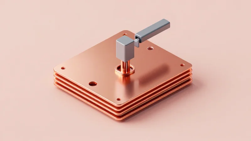
Fabricating high-current PCBs with copper weights exceeding 3oz demands a departure from standard manufacturing processes. The primary hurdle lies in the etching cycle; as the copper thickness increases, the chemical etchants require significantly longer exposure times. This extended immersion often leads to 'under-etching' or 'lateral erosion' of the copper trace edges, which can compromise impedance control and geometric precision.
Managing Side-Wall Profile and Undercut
The cross-sectional profile of a heavy copper trace is rarely rectangular. Due to the isotropic nature of traditional spray etching, the top corners of a trace are exposed to the etchant longer than the base, resulting in a trapezoidal shape. Maintaining a controlled etch factor is critical to ensuring that the base width is sufficient to carry the rated current without excessive temperature rise.
| Challenge | Impact | Mitigation Strategy |
|---|---|---|
| Extended Etch Time | Excessive Lateral Undercut | Advanced Photoresist & Specialized Chemistry |
| High Aspect Ratio | Plating Voids in Vias | High-Aspect-Ratio Plating Cycles |
| Copper Distribution | Uneven Etching Rates | Copper Balancing & Thieving Patterns |
Fabrication FAQ
- Why is trace spacing larger for heavy copper?
Due to the depth of the copper, manufacturing clearances must be increased to account for the lateral etch characteristic; tighter spaces risk bridging during the prolonged chemical immersion process. - What is the impact of heavy copper on solder mask application?
Thick traces create significant 'steps' on the board surface. Standard solder mask may not provide adequate coverage over these high profiles, often requiring multiple passes or specialized high-build liquid photoimageable (LPI) masks to prevent oxidation. - Does heavy copper affect hole wall integrity?
Yes, plating in high-aspect-ratio holes becomes difficult with heavy copper. Fabricators must utilize specialized pulse-plating techniques to ensure uniform copper deposition within the barrel of the hole without creating 'dog-bone' plating defects.
Reliability and Stress Analysis
Managing CTE Mismatch and Thermal Cycling
High-current motor drive applications generate significant thermal cycling, which subjects the PCB to mechanical stress due to the Coefficient of Thermal Expansion (CTE) differential between the FR-4 dielectric and the thick copper traces. As copper expands faster than the laminate, cyclic loading can lead to barrel cracking in plated through-holes (PTHs) and trace peeling. To mitigate this, engineers must prioritize high-Tg (glass transition temperature) laminates with low Z-axis expansion coefficients and utilize balanced copper distribution to neutralize internal mechanical stresses.
Comparison of Thermal Management Strategies
| Strategy | Primary Benefit | Risk Mitigation |
|---|---|---|
| High-Tg Laminate | Maintains structural integrity above 170°C | Prevents delamination during reflow |
| Balanced Copper Stacks | Equalizes mechanical tension | Reduces board warping/bowing |
| Thermal Vias | Efficient heat dissipation | Lowers hotspot temperatures |
Preventing Delamination and Fatigue
Delamination is often the result of insufficient bonding strength between the thick copper surface and the substrate. During high-current operation, local temperature spikes can weaken the adhesive interface. Adhering to strict IPC-6012 standards regarding foil roughness and surface treatments is essential. Furthermore, large copper pours should be cross-hatched or partitioned where electrical requirements allow to reduce the net surface area subjected to shear stress, thereby enhancing the overall structural reliability of the motor drive circuit.
Frequently Asked Questions
- Why does CTE mismatch cause barrel cracking?
Because copper expands at a different rate than the substrate, the vertical movement in the barrel of a through-hole creates tension that eventually fractures the plating if the cycle count is high. - What is the recommended Tg for motor drives?
For high-current applications, a Tg of 170°C or higher is recommended to maintain the laminate's physical properties under sustained thermal load. - Does trace width influence stress accumulation?
Yes; excessively wide copper traces without thermal relief or proper distribution increase the internal force exerted on the substrate during expansion.
Design for Manufacturing (DFM) Best Practices
Design for Manufacturing (DFM) Best Practices
Successful integration of thick copper PCBs requires aligning design geometry with the limitations of chemical etching and mechanical plating. Designers must prioritize copper distribution and feature spacing to ensure uniform thermal dissipation and structural integrity under high-current loads.
Copper Balancing and Etch Compensation
Asymmetric copper distribution is the primary cause of board warpage during lamination and reflow. To maintain structural stability, designers should distribute copper symmetrically across board layers. Furthermore, because etching thick copper (3oz or higher) involves prolonged exposure to chemical baths, feature widths must be overcompensated to account for lateral undercutting of the trace sidewalls.
| Copper Weight (oz) | Minimum Trace Width | Typical Etch Factor |
|---|---|---|
| 2 oz | 0.25 mm | 1:1 |
| 3 oz | 0.40 mm | 0.8:1 |
| 4 oz+ | 0.65 mm | 0.5:1 |
Hole Plating and Thermal Management
High-current interconnects rely on robust through-hole plating to carry electricity between layers without excessive heat generation. Specify a minimum of 25 µm (1 mil) of copper in the hole barrel to prevent barrel cracking under thermal cycling. For extreme currents, consider using conductive vias or 'via stitching' to parallelize the current path, thereby reducing individual via stress.
Solder Mask Application Guidelines
- Why is solder mask application difficult on thick copper?
The significant height difference between thick traces and the board substrate makes it difficult for liquid photoimageable solder mask (LPI) to achieve uniform coverage, often leading to air entrapment or thin spots on sidewalls. - What is the recommended solution?
Utilize a high-build solder mask process or multiple printing passes to ensure full coverage over the trace edges, preventing potential solder bridging during assembly.
Selecting the optimal copper weight for your motor drive is a balancing act of physics and manufacturing reality. By prioritizing thermal headroom and adhering to IPC standards, you ensure that your design remains resilient under the most grueling conditions. Are you ready to optimize your power stage for maximum efficiency? Contact our engineering team today to review your board specifications.
