
High-amperage power circuits demand more than just standard board fabrication; they require a sophisticated understanding of material science and geometric limitations. When designing for 3oz to 6oz copper weights, standard DFM assumptions fall apart, leading to thermal failure and manufacturing defects. This guide provides the technical blueprint to ensure your high-power designs translate flawlessly from schematic to finished board.
The Physics of Heavy Copper: Understanding Current Capacity
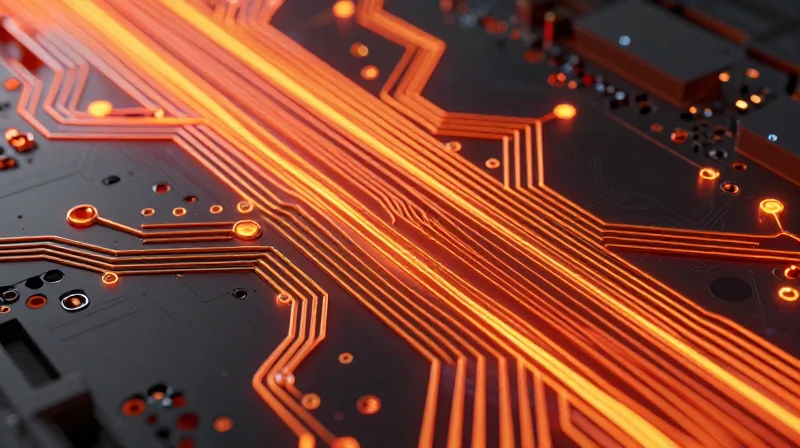
The Thermal Dynamics of Thick Copper
When utilizing 3oz to 6oz copper weights, the primary design challenge is managing the heat generated by resistive losses ($I^2R$). Unlike standard 1oz boards, thick copper significantly reduces DC resistance, allowing for higher current density; however, the increased mass alters the thermal equilibrium of the PCB. Designers must account for the fact that heat dissipation is no longer purely a function of surface convection, but also internal thermal conductivity within the massive copper traces.
Key Variables in Current Capacity
| Variable | Influence on Capacity | Design Consideration |
|---|---|---|
| Copper Weight | Direct (Positive) | Increasing thickness reduces cross-sectional resistance. |
| Trace Width | Direct (Positive) | Widening traces dissipates heat across a larger area. |
| Temperature Rise | Inverse | Higher allowable T-rise permits higher nominal current. |
| Substrate CTE | Constraint | Thick copper expands differently than FR4, risking barrel cracking. |
Physics-Based Design FAQ
- How does copper weight affect current density?
Doubling copper weight essentially doubles the cross-sectional area, which cuts resistance in half for a given width, effectively allowing higher current flow at the same thermal threshold. - Why do 6oz boards require specific stack-up planning?
The massive thermal mass of 6oz copper necessitates controlled impedance and balanced copper distribution to prevent warping and ensure uniform thermal dissipation across the board surface. - What is the role of surface area in heat dissipation?
Current capacity is limited by the ability of the trace to shed heat into the environment; larger surface areas increase convective cooling, preventing premature degradation of the PCB material.
Trace Width and Spacing: Avoiding Etching Limitations
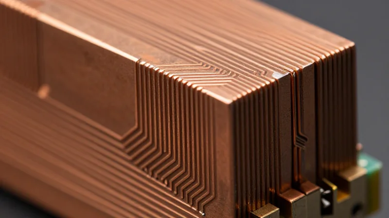
Managing Lateral Etching and Undercutting
When using copper weights between 3oz and 6oz, the primary manufacturing challenge is the extended dwell time required in the etching bath. Because the etchant attacks the copper vertically and horizontally simultaneously, thick copper suffers from significant 'undercutting'—the erosion of the base of the trace beneath the photoresist. If the trace width is insufficient, this lateral erosion can compromise structural integrity, leading to trapezoidal trace cross-sections that reduce current-carrying capacity and mechanical adhesion to the substrate.
Design Guidelines for Thick Copper Spacing
To mitigate manufacturing defects, designers must increase minimum spacing requirements significantly beyond standard 1oz copper specifications. The general rule of thumb for heavy copper is to maintain a spacing-to-thickness ratio that allows the etchant to clear the gaps without over-processing the circuit features.
| Copper Weight | Min. Trace Width | Min. Spacing (Clearance) |
|---|---|---|
| 3oz (105µm) | 15 mil | 15 mil |
| 4oz (140µm) | 20 mil | 20 mil |
| 6oz (210µm) | 30 mil | 30 mil |
Critical DFM Considerations
- How does etching time impact trace geometry?
Thick copper requires longer exposure to etchant, which increases the amount of material removed from the sides. This causes a tapered profile, reducing the effective copper cross-sectional area compared to thin copper. - Why must I increase clearance beyond standard limits?
Tight spacing leads to 'etch bridging' where copper residues remain trapped between features, causing potential short circuits that are difficult to detect during standard AOI. - Should I use square or rounded trace pads?
Avoid sharp 90-degree corners on thick copper traces, as they are prone to acid trapping during etching and can act as stress concentrators during thermal cycling.
Mastering Via Reliability and Plating Thickness
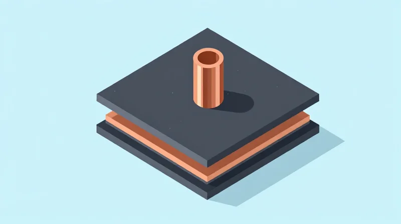
In high-current PCB applications, vias are not merely vertical interconnections; they are high-stress bottlenecks. When dealing with copper weights of 3oz and above, standard through-hole plating processes are often inadequate. Achieving consistent, thick copper on the inner walls of the barrel is mandatory to prevent fracture due to the coefficient of thermal expansion (CTE) mismatch between the copper barrel and the FR-4 laminate during extreme thermal cycling.
Requirements for Hole Wall Reliability
The primary challenge in high-current thick copper design is ensuring a minimum plating thickness of 25 micrometers (1 mil) within the via barrel. Standard plating cycles designed for 0.5oz or 1oz copper will result in 'barrel cracking' when subjected to the high amperage surges typical of power distribution systems. Designers must specify higher class fabrication standards to ensure robust chemical deposition before the final plating phase.
| Copper Weight | Target Hole Wall | Reliability Risk |
|---|---|---|
| 3oz | 25-30um | Moderate thermal cycling stress |
| 6oz | 35um+ | High risk of barrel fracture |
Advanced Plating Techniques
To achieve superior reliability, fabricators utilize specialized electrolytic pulse-plating processes. This method promotes uniform copper deposition throughout the entire length of the hole, preventing the typical 'dog-boning' effect where plating is thicker at the hole edges and thinner in the center. For critical high-current paths, utilizing larger via diameters or arrays of vias is recommended to lower the total contact resistance.
FAQs on Thick Copper Via Design
- Can I use standard via sizes for 6oz copper?
No, standard small-diameter vias struggle with chemical circulation during deep-hole plating, leading to voids. Use larger drill diameters to ensure adequate plating solution flow. - Why is CTE mismatch a critical failure point?
Copper and FR-4 expand at significantly different rates. In heavy copper designs, the massive copper barrel exerts extreme tensile force on the hole walls during heating, leading to circumferential cracks. - Is via filling required?
For extreme current applications, conductive or non-conductive epoxy via filling and capping is recommended to provide structural reinforcement to the via barrel.
Thermal Management and Heat Sinking Techniques
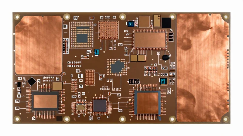
Optimizing Copper Pours for Heat Spreading
In 3oz-6oz designs, copper pours function as massive heat sinks. Unlike signal-layer copper, thermal pours should be kept as contiguous as possible to maximize surface area. To prevent uneven etching, use a cross-hatched pattern if the copper coverage exceeds 80% on a specific layer, though solid planes are preferred for maximum thermal dissipation if your fabricator can accommodate the necessary etching compensation.
Thermal Relief and Assembly Considerations
Using standard thermal relief patterns for high-current components often acts as a bottleneck, creating excessive localized resistance. For 3oz+ copper, replace standard narrow 'spokes' with solid or direct-connect pads to ensure the heat flows effectively into the plane. Note that this requires high-power soldering equipment during assembly to overcome the increased thermal mass.
| Feature | Standard Copper | Heavy Copper (3oz-6oz) |
|---|---|---|
| Connection Type | Thermal Spokes | Direct/Solid Connect |
| Pour Pattern | Solid Planes | Balanced/Cross-hatched |
| Via Usage | Standard Thermal Vias | Plated-up Thermal Stacks |
FAQ: Thermal Design Best Practices
- Should I use thermal vias in 6oz copper?
Yes, but prioritize large-diameter vias (0.5mm+) with thick wall plating to act as thermal conduits between internal and external layers. - How does heavy copper affect reflow soldering?
Heavy copper acts as a massive heat sink, often leading to 'cold solder' joints. Increasing the profile soak time is essential for successful reflow. - Can I use thermal reliefs on high-current MOSFET pins?
Avoid them. High-current paths require maximum copper cross-section; thermal reliefs introduce unnecessary parasitic resistance and failure points.
Surface Finish Considerations for High Power Circuits
For 3oz to 6oz copper designs, the surface finish must do more than prevent oxidation; it must provide a robust foundation for heavy-duty solder joints that experience significant thermal expansion. The primary challenge is balancing planar uniformity for surface-mount devices against the structural requirements for power-handling components.
Comparison of Surface Finishes for Heavy Copper
| Surface Finish | Thermal Performance | Solder Joint Reliability | Process Suitability |
|---|---|---|---|
| HASL (Lead-Free) | Moderate | High (Good for massive joints) | Difficult on high-aspect vias |
| ENIG | Excellent | Moderate (Nickel-brittleness risk) | Best for fine pitch |
| Immersion Silver | Good | High | Good planar finish |
| ENEPIG | Superior | Very High | Optimal for power/thermal |
Critical Factors for High-Current Joints
When dealing with 3oz-6oz copper, standard finishes like HASL can sometimes lead to uneven surfaces that create solder bridging or poor wetting on thermal pads. For power-intensive applications, chemical-based finishes that offer high planarity, such as ENEPIG, are often preferred over traditional hot-air leveling due to the extreme heat-sink requirements of the board.
Frequently Asked Questions
- Why is ENIG problematic for high-power connections?
ENIG can introduce nickel-layer brittleness under extreme thermal cycling, potentially leading to fractures in large power-component solder joints. - Is HASL recommended for 6oz copper designs?
HASL is generally discouraged for heavy copper because it creates significant unevenness, making it difficult to mount large power components flatly across the copper pour. - What is the best balance for cost and reliability?
Immersion Silver provides a highly planar surface with excellent solderability, making it a cost-effective choice for many high-current applications that do not require the gold protection of ENEPIG.
The Impact of Solder Mask and Silkscreen on Thick Copper
Topography and Solder Mask Coverage
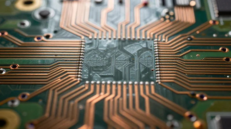
When utilizing 3oz to 6oz copper, the extreme trace height creates a significant vertical topography challenge. Standard solder mask application methods often fail to adequately coat the sidewalls of these tall traces, leading to exposed copper, oxidation, or potential electrical shorts. For high-current designs, designers must specify 'Liquid Photoimageable (LPI) solder mask' with double-pass applications to ensure the valleys between traces are filled and sidewalls are fully insulated.
Mitigating Solder Bridge Risks
The gap between thick copper traces is prone to solder bridging during reflow due to the reservoir effect of large traces. To maintain structural integrity and prevent shorts, incorporate the following DFM strategies:
- Solder Mask Dam
Increase the solder mask dam width to a minimum of 0.15mm (6 mil) between fine-pitch pads, as the height of the copper makes standard registration tolerances insufficient. - Trace Clearance
Increase air gaps between high-potential traces to compensate for mask 'slump' over the edges of thick copper. - Silkscreen Constraints
Avoid printing silkscreen over high-current copper areas; the thickness differential can cause the ink to smear or result in brittle, flaking legends that introduce contaminants.
| Design Factor | 3oz Copper Strategy | 6oz Copper Strategy |
|---|---|---|
| Mask Application | Single or Double Pass | Mandatory Double Pass |
| Min. Mask Dam | 0.125mm | 0.200mm |
| Silkscreen Placement | Keep clear of high-current paths | Prohibited on copper planes |
Silkscreen Best Practices for Heavy Copper
Because thick copper creates a non-planar surface, silkscreen ink will not adhere uniformly. Printing over a height difference of 100 microns or more leads to broken text, poor resolution, and potential ink entrapment in narrow corners. Always define a 'Keep-out' zone for silkscreen around high-current traces to maintain PCB cleanliness and avoid interference with solder paste deposition or automated optical inspection (AOI).
Advanced DFM Checklists for Motor Drive Reliability

Critical DFM Audit for Motor Drive High-Current Stages
Reliability in motor drive applications hinges on the mechanical integrity of high-current paths. Before production release, engineers must verify that the copper weight does not induce parasitic effects or solderability failures. The following checklist addresses the specific challenges associated with heavy copper geometries in power electronics.
- Via Stitching and Barrel Integrity
Ensure that high-current paths utilizing multiple layers are stitched with an adequate number of vias to prevent current crowding. Vias must have sufficient plating thickness (typically 1oz-2oz wall thickness) to withstand repetitive thermal cycling. - Trace-to-Edge and Pad Clearances
Thick copper requires increased routing clearances. Maintain a minimum gap of 1.5x the copper thickness to prevent bridging during the etching process and to ensure electrical isolation at high operating voltages. - Thermal Relief Optimization
Standard thermal reliefs are often insufficient for 3oz+ copper. Use wide, direct thermal connections to pads to ensure low-resistance paths, while balancing this against the risk of cold solder joints during reflow. - Solder Mask Dam Stability
With 3oz+ copper, the physical height of traces makes solder mask application difficult. Ensure that mask dams between fine-pitch pads are at least 0.15mm wide to prevent solder bridging under high-vibration conditions.
DFM Verification Matrix for Heavy Copper
| Parameter | 3oz Copper Limit | 6oz Copper Limit | Critical Concern |
|---|---|---|---|
| Min Trace Width | 0.25mm | 0.50mm | Etch undercut |
| Min Air Gap | 0.30mm | 0.60mm | Arcing/Isolation |
| Via Diameter | 0.40mm | 0.60mm | Plating thickness |
Finally, ensure that all high-current power stages are physically separated from sensitive signal circuitry. Cross-talk and EMI generated by high-switching frequency motor drives can destabilize gate drivers if the copper weight is not managed with proper return path impedance and physical isolation.
Successfully deploying high-current systems depends entirely on how well your board handles power density. By integrating these specific DFM rules into your design workflow, you mitigate common failure points and extend the lifespan of your motor drive electronics. Ready to optimize your next project? Contact our engineering team today for a comprehensive DFM review of your thick copper design.
