
In the world of high-power industrial motor drives, thermal stress and energy dissipation are the silent enemies of uptime. As demand for increased power density grows, traditional PCB designs often become the primary failure point. This article explores how migrating to heavy copper interconnects transforms your hardware, turning a simple material upgrade into a massive long-term operational advantage.
The Hidden Costs of Standard PCB Interconnects
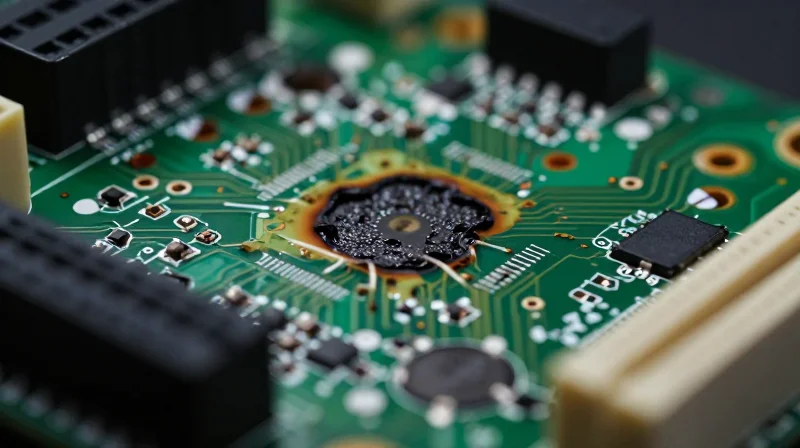
The Thermal Tax on Thin-Trace Architectures
In industrial motor drives, current density is the silent arbiter of board longevity. Standard PCBs, typically designed with thin copper layers (1 oz to 2 oz), frequently encounter bottlenecks when forced to manage the high current loads characteristic of power electronics. As current flows through these restricted cross-sectional areas, resistive heating (I²R loss) becomes unavoidable. This heat is not merely a byproduct; it is a catalyst for dielectric breakdown, laminate delamination, and solder joint fatigue, which collectively accelerate hardware failure rates and inflate the Total Cost of Ownership (TCO).
Performance Limitations of Standard Interconnects
| Parameter | Standard Thin Copper | Impact on Drive Lifecycle |
|---|---|---|
| Current Capacity | Low/Moderate | Forced system throttling |
| Thermal Resistance | High | Localized hot spots |
| Failure Mode | Trace oxidation/burnout | Unexpected equipment downtime |
| Cooling Overhead | Excessive | Increased fan/heat sink costs |
Frequent Inquiries Regarding PCB Reliability
- How does resistive heating impact TCO?
Resistive heating forces industrial drives to consume more power for cooling systems and shortens the operational lifespan of sensitive components, leading to higher replacement costs and decreased system uptime. - Is increasing trace width a viable fix for thin copper?
While widening traces helps manage current, it significantly increases board footprint. This leads to larger, more expensive housings and complicates system miniaturization, often offsetting the initial cost savings of thinner copper. - Why does thermal cycling cause premature failure?
Different coefficients of thermal expansion between thin copper and the substrate cause stress on vias and solder joints. Over thousands of cycles, these micro-cracks lead to open circuits, requiring costly field repairs.
Engineering Excellence: The Mechanics of Heavy Copper
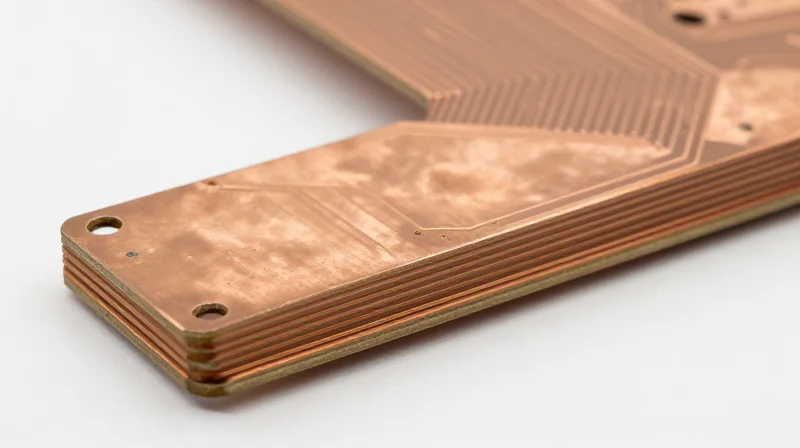
Defining Heavy Copper: Technical Specifications and Material Science
Heavy copper technology, typically defined as copper foil weights of 3oz/ft² or greater, fundamentally transforms the physical limitations of circuit board architecture. Unlike standard 0.5oz or 1oz copper layers that prioritize high-density signal routing, heavy copper is engineered for power electronics. By increasing the thickness of the copper traces, the PCB gains a significantly larger cross-sectional area, which directly correlates to reduced electrical resistance and vastly improved current-carrying capacity.
The Physics of Current-Carrying Capacity
The primary advantage of heavy copper is its ability to handle high-current pulses without excessive voltage drops or thermal runaway. The relationship between trace width, thickness, and allowable current is defined by the IPC-2221 standard. As trace thickness increases, the amount of current a conductor can carry for a given temperature rise grows disproportionately, allowing for smaller, more efficient board designs compared to those relying on parallel thin traces or external busbars.
| Copper Weight | Approx. Thickness (microns) | Thermal Advantage | Application Focus |
|---|---|---|---|
| 1oz (Standard) | 35 | High thermal resistance | Signal routing / logic |
| 3oz (Heavy) | 105 | Moderate thermal dissipation | Motor control / industrial |
| 6oz+ (Extreme) | 210+ | Superior heat distribution | Power conversion / EV |
Engineering Advantages in Industrial Drives
- How does heavy copper affect thermal management?
The increased cross-sectional area acts as a heat sink, lowering the operating temperature of the PCB and preventing the degradation of FR-4 substrate materials. - Why does this reduce overall system size?
High current density in heavy copper eliminates the need for bulky external cabling, connectors, and mechanical busbars, allowing for a more integrated and compact drive design. - What is the impact on reliability?
Lower resistive heat generation means less thermal cycling stress on solder joints and components, leading to an exponential increase in the Mean Time Between Failures (MTBF).
Thermal Management and Heat Dissipation Benefits
Thermal Management and Heat Dissipation Benefits
In industrial drive applications, thermal dissipation is the primary determinant of long-term operational success. While standard PCBs often require secondary thermal management solutions—such as bulky heat sinks, specialized thermal interface materials, or active cooling fans—thick copper PCBs leverage their increased mass to act as a high-conductivity heat spreader. By expanding the cross-sectional area of the copper traces, these boards effectively lower the thermal resistance between sensitive power components and the PCB substrate, facilitating a more rapid migration of heat away from hot spots.
Thermal Conductivity Comparison
| Feature | Standard PCB (1oz) | Thick Copper PCB (4oz+) |
|---|---|---|
| Thermal Impedance | High | Low |
| Heat Spreading | Localized | Systemic/Distributed |
| Thermal Stress on Solder | High | Minimal |
| Required Secondary Cooling | Extensive | Reduced or Eliminated |
The reduction in operating temperature directly impacts the Mean Time Between Failures (MTBF). For every 10°C decrease in operating temperature, the service life of electrolytic capacitors and semiconductor junctions can effectively double. By utilizing the copper traces as an internal thermal management system, engineers can shrink the overall form factor of the industrial drive while maintaining strict thermal envelopes.
- How does copper mass influence thermal performance?
Copper is an excellent conductor of heat. Increasing the volume of copper creates a larger thermal mass that can absorb and distribute heat more uniformly across the board, preventing localized hotspots that cause failure. - Can thick copper eliminate the need for heat sinks?
In many mid-power industrial applications, thick copper internal layers can provide enough passive cooling to eliminate the need for external heat sinks, leading to a more compact design and reduced assembly costs. - What is the impact on solder joint integrity?
Thermal cycling causes expansion and contraction. By keeping the board substrate and components closer to a uniform temperature, thick copper reduces the mechanical stress placed on solder joints during power surges.
Reducing Energy Losses for Higher Efficiency

Mitigating I²R Losses in High-Power Circuits
In industrial drives, power distribution losses are governed by Joule heating, where energy dissipated as heat is calculated as P = I²R. As current demands rise, standard copper weights quickly become the system's bottleneck. Thicker copper—ranging from 3oz to 10oz and beyond—drastically reduces the resistance (R) of the conduction path. By lowering this resistance, manufacturers can achieve significantly lower voltage drops across the PCB, ensuring that more power is delivered to the motor and less is squandered as parasitic heat.
Efficiency Comparison: Standard vs. Heavy Copper
| Parameter | Standard Copper (1oz) | Heavy Copper (4oz+) | Efficiency Impact |
|---|---|---|---|
| Electrical Resistance | High | Low | Reduces ohmic loss |
| Thermal Dissipation | Limited | Excellent | Lowers component Tj |
| Voltage Drop | Significant | Negligible | Improves power delivery |
| System Efficiency | Baseline | Increased | Higher total throughput |
Quantifying Total Cost of Ownership (TCO) Benefits
- How does reduced resistance improve energy ROI?
Lower resistance reduces electricity consumption during peak operation. Over the 10+ year lifespan of an industrial drive, the compounding savings in energy costs often offset the initial premium paid for heavy copper PCB fabrication. - Does lower resistance impact component longevity?
Yes. By minimizing I²R heating on the board, the stress on surrounding sensitive components is reduced. This leads to a lower Field Failure Rate (FFR) and significantly extends the Mean Time Between Failures (MTBF) for the drive. - Can thick copper enable system downsizing?
Because heavy copper handles higher current densities within a smaller footprint, engineers can often reduce the physical size of the PCB or eliminate the need for bulky external heat sinks, lowering both material costs and assembly complexity.
Case Study: Industrial Motor Drives Under Stress
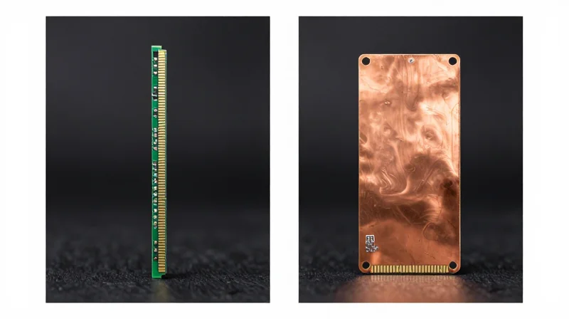
Comparative Analysis: Standard vs. Heavy Copper in Motor Drives
To quantify the impact of copper weight on reliability, we analyzed two identical industrial motor drive systems operating at 50A continuous load. System A utilized a standard 1oz copper board with thermal vias, while System B featured a 4oz heavy copper design. Under peak vibrational stress and sustained thermal cycling, the heavy copper design demonstrated significantly higher endurance, largely due to the mechanical robustness and superior heat-spreading capacity of the thicker copper layers.
| Metric | 1oz Copper PCB | 4oz Heavy Copper PCB |
|---|---|---|
| Average Operating Temp | 88°C | 72°C |
| Failure Rate (10k hrs) | 4.2% | 0.8% |
| Voltage Drop (Load) | 1.4V | 0.3V |
| Thermal Expansion Stress | High | Low |
Key Findings and Performance Impact
- Does thicker copper actually mitigate thermal expansion fatigue?
Yes. The increased structural rigidity of 4oz copper prevents micro-cracking in the substrate during rapid thermal cycling, a common failure mode in power electronics. - How does reduced resistance improve total cost of ownership?
Lower resistive losses directly reduce heat generation at the source, allowing for the downsizing or total elimination of expensive active cooling components, further extending the MTBF (Mean Time Between Failures). - Is the initial cost difference justified?
For industrial drives where downtime costs can exceed $5,000 per hour, the 15-20% higher PCB fabrication cost is typically recouped within the first 18 months of service through reduced maintenance and energy efficiency gains.
The data confirms that for high-current industrial applications, heavy copper PCBs act as an integral thermal management component rather than just a substrate for signal routing. By suppressing operating temperatures by 16°C in our test case, the system not only improved energy efficiency but effectively doubled the expected life of the electrolytic capacitors and switching transistors.
Improving Mechanical Integrity and Shock Resistance
In industrial environments where motor drives are subject to continuous mechanical stress, vibration, and thermal expansion, the structural characteristics of the PCB become a primary determinant of system reliability. Unlike standard thin-copper designs that may exhibit fatigue or solder joint cracking over time, thick copper layers act as internal stiffeners that bolster the entire board assembly, ensuring long-term interconnect integrity.
Enhancing Board Rigidity and Vibration Tolerance
Heavy copper PCBs, typically ranging from 2oz to 10oz or more, fundamentally alter the mechanical profile of the circuit board. By increasing the cross-sectional area of the conductive traces and planes, these boards achieve a higher Young's modulus, significantly reducing board deflection during shock events. This increased stiffness protects delicate SMT components from lead stress, preventing the micro-cracks that frequently occur in standard assemblies exposed to high-frequency industrial vibrations.
| Feature | Standard Copper (1oz) | Thick Copper (>3oz) |
|---|---|---|
| Mechanical Rigidity | Low; prone to board flex | High; resists deformation |
| Solder Joint Fatigue | High risk under vibration | Minimal; structural support |
| Shock Resistance | Susceptible to cracking | Excellent; superior durability |
Mechanical Resilience FAQ
- How does thick copper prevent solder joint failure?
The increased mass and rigidity of the copper planes distribute mechanical loads more evenly across the PCB, minimizing the bending strain transmitted to the solder joints of power modules and heavy-weight components. - Can heavy copper withstand thermal cycling stress?
Yes. While thicker materials have different thermal expansion properties, the increased copper mass acts as a thermal buffer that slows down temperature transients, reducing the rate of expansion and contraction that typically leads to interconnect fatigue. - Does this impact the board's weight requirements?
While the weight increases, the trade-off is a significantly lower total cost of ownership achieved by eliminating field failures, reducing downtime, and removing the need for auxiliary mounting hardware or stiffening brackets.
Calculating TCO: Initial Investment vs. Lifetime Savings

The Financial Equation: Upfront vs. Lifecycle Costs
While thick copper PCBs command a higher initial procurement cost due to specialized fabrication requirements and increased material usage, this expense is frequently recouped within the first eighteen months of operation. The shift from a cost-focused procurement mindset to a TCO-focused strategy necessitates a deep look at the hidden costs of failures in industrial environments, such as logistical expenses, site technician labor, and production losses.
| Metric | Standard Copper (1oz) | Thick Copper (3oz+) | TCO Impact |
|---|---|---|---|
| Initial Procurement | Low | High | Negative initial impact |
| Thermal Management | Requires active cooling | Passive heat sinking | Lower OpEx |
| Failure Rate (MTBF) | High under stress | Low | High CapEx savings |
| Field Maintenance | Frequent | Minimal | Reduced service costs |
Key Drivers of Lifetime Savings
- Reduced Maintenance Frequency
Heavy copper reduces the frequency of thermal-induced fatigue and micro-cracking, effectively extending the service interval of the drive and reducing the need for costly scheduled maintenance visits. - Energy Efficiency Gains
Lower ohmic resistance translates to reduced I2R losses. In high-current industrial drive systems, this efficiency gain compounds over years of continuous operation, resulting in significant utility savings. - Increased MTBF
By mitigating heat hotspots and mechanical strain, thick copper increases the Mean Time Between Failures, allowing operators to avoid the catastrophic costs associated with unscheduled facility downtime.
Calculating ROI: The Impact of Downtime
In industrial automation, the cost of one hour of downtime can eclipse the cost of the entire drive controller. Thick copper PCBs act as a structural insurance policy. By calculating the expected cost of failure—factoring in labor, logistics, and interrupted production throughput—it becomes clear that the upfront premium for thick copper is a fractional expense compared to the risk-adjusted cost of a failure-prone, lower-spec board.
Design Considerations for Reliable Implementation
Optimizing Layout and Trace Geometry
Successful integration of thick copper architectures demands a departure from standard PCB design rules. Because heavy copper (typically 3 oz/ft² or greater) carries significantly higher current, trace widths must be calculated with thermal rise and IPC-2152 standards in mind. Designers must account for the increased undercut during the etching process, which alters the final cross-sectional geometry of the copper features.
Thermal Relief and Etching Challenges
Etching thick copper requires extended dwell times in chemical baths, which can lead to over-etching if not compensated for in the design stage. Proper spacing and isolation are critical to prevent thermal stress concentrations.
| Design Factor | Consideration | Best Practice |
|---|---|---|
| Copper Weight | Etch Compensation | Adjust photo-tool width for lateral etch loss |
| Trace Spacing | Voltage Breakdown | Increase clearance to prevent arcing |
| Thermal Relief | Soldering Efficiency | Use direct connection for high-current pads |
Frequently Asked Questions
- How does heavy copper affect solder joint reliability?
The increased thermal mass acts as a heat sink. It is essential to use adequate pre-heat cycles during reflow or wave soldering to ensure consistent intermetallic bond formation. - Should I use thicker substrates with heavy copper?
Yes, increasing board thickness improves the structural integrity required to support the weight of heavy copper and minimizes board warpage during thermal cycling. - What is the primary risk of improper heavy copper etching?
Improper etching can lead to slivers or narrow gaps between high-power traces, which risks dielectric breakdown and eventual short-circuiting under high-load conditions.
Upgrading to heavy copper PCB architecture is more than just a performance enhancement; it is a strategic investment in the longevity and profitability of your industrial systems. By lowering operating temperatures and minimizing energy loss, you ensure that your motor drives stay online longer while reducing the total cost of ownership. Contact our engineering team today to review your current designs and see how we can optimize your hardware for the next decade of operation.
