
The demand for rapid, decentralized healthcare is pushing in vitro diagnostics (IVD) into the palm of the patient’s hand. As diagnostic devices shrink, the engineering challenges surrounding PCB design have reached a breaking point. We explore why traditional signal processing architectures are being outpaced and how new material innovations are setting the standard for the next generation of precision diagnostics.
The Evolution of IVD: From Benchtop to Point-of-Care
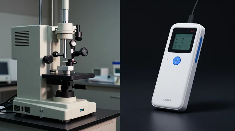
Historically, diagnostic testing relied on large, climate-controlled benchtop analyzers that required significant power, fluidic handling, and expert operation. As healthcare moves toward decentralized models, the industry is pivoting toward Point-of-Care (POC) devices. This shift necessitates a fundamental redesign of signal processing architectures, moving away from legacy discrete component layouts toward highly integrated, application-specific hardware that can operate in non-traditional environments.
The Engineering Challenge: Scaling Down
Miniaturization introduces significant signal-to-noise ratio (SNR) challenges. In traditional laboratory settings, bulky analog-to-digital converters and dedicated shielded cabling mitigate interference. In POC devices, the hardware must perform similarly while shrinking the footprint by orders of magnitude. This necessitates a strategic move toward innovative PCB materials with superior dielectric properties and lower signal loss, compensating for the lack of traditional physical shielding.
| Parameter | Benchtop Architecture | Point-of-Care (POC) Architecture |
|---|---|---|
| Integration | Modular/Discrete | SoC/SiP High Integration |
| Signal Path | Shielded Cabling | Controlled PCB Traces |
| Thermal Management | Active Cooling/Fans | Passive Dissipation/Materials |
| Power Source | Mainline/Grid | Battery-Optimized |
Key Considerations for Next-Generation IVD
- How do PCB materials influence diagnostic sensitivity?
Advanced substrate materials minimize parasitic capacitance and dielectric loss, which is essential for detecting the minute electrical signatures generated in bio-sensors without external amplification artifacts. - Why shift away from traditional signal processing?
Legacy architectures consume too much power and board space for portable units; modern System-on-Chip (SoC) architectures allow for real-time edge processing, reducing data latency and energy requirements. - What is the role of signal integrity in POC devices?
In portable IVD, the integrity of the raw analog signal is paramount, as software post-processing cannot fully compensate for poor signal conditioning at the front-end interface caused by suboptimal PCB layout or material choices.
Traditional PCB Architectures: Limitations in a Shrinking Landscape
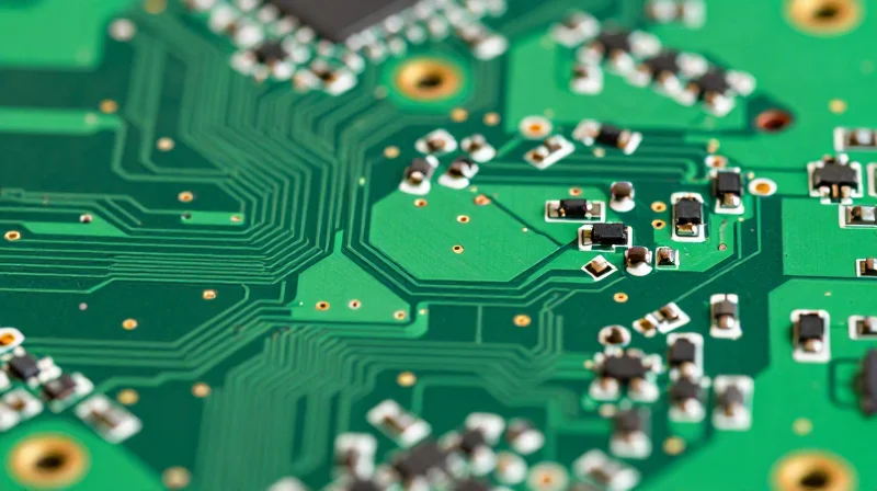
The Bottlenecks of Legacy PCB Architectures in IVD
As In-Vitro Diagnostic (IVD) systems migrate from massive laboratory benches to compact point-of-care (POC) handheld units, traditional Printed Circuit Board (PCB) architectures have reached their functional ceiling. The core challenge lies in the reliance on standard FR-4 substrates and legacy manufacturing processes which were not originally optimized for the high-frequency, heat-sensitive, and space-constrained requirements of modern molecular diagnostics.
Critical Performance Deficits
| Limitation Factor | Legacy Architecture Impact | Result in IVD Applications |
|---|---|---|
| Thermal Dissipation | Low thermal conductivity of glass-epoxy | Component drift and reduced sensor accuracy |
| Signal Integrity | High dielectric loss at high frequencies | Attenuation of sensitive biochemical signal data |
| EMI Susceptibility | Inadequate shielding in high-density layouts | False positives in ultra-low signal detection |
| Physical Scaling | Limited layer density and trace width | Inability to integrate complex microfluidic controls |
Frequent Questions Regarding Legacy Architecture Failure
- Why does thermal management fail in compact IVD devices?
Traditional PCBs use FR-4, which acts as a thermal insulator. In a confined POC housing, the heat generated by signal processing chips cannot escape, causing thermal expansion that affects the precision of microfluidic flow sensors. - How does EMI specifically interfere with IVD results?
Modern IVD diagnostics rely on measuring minute electrical or optical changes. Traditional PCB layouts lack the advanced integrated shielding required to protect these high-impedance circuits from internal digital noise, leading to degraded signal-to-noise ratios. - Why can't we simply decrease trace sizes on current materials?
While shrinking traces is physically possible, the dielectric constant and dissipation factor of standard substrates result in significant signal attenuation at high speeds, compromising the data transmission required for real-time diagnostic reporting.
The Material Revolution: Advancements in Dielectric Constants

The Material Revolution: Advancements in Dielectric Constants
As IVD devices transition toward increasingly compact form factors, the dielectric properties of PCB substrates have become the critical bottleneck for signal integrity. Modern high-frequency diagnostic sensors rely on precise data acquisition that legacy materials like FR-4 often fail to support due to excessive signal dissipation and parasitic capacitance. The shift toward ultra-low loss (ULL) laminates and specialized PTFE-based substrates addresses these challenges by maintaining consistent dielectric constants across varying frequencies and temperatures.
Engineering Impact on Signal Integrity
The dielectric constant (Dk) and dissipation factor (Df) are the primary determinants of electrical performance. By employing advanced thermoset resin systems and ceramic-filled composites, engineers can achieve a lower, more stable Dk, which reduces signal propagation delay and attenuation. These advancements are essential for the high-speed processing required in real-time electrochemical biosensing and optical diagnostic modalities.
| Parameter | Legacy FR-4 | Advanced Laminates | Diagnostic Benefit |
|---|---|---|---|
| Dk Stability | Variable | Highly Stable | Phase Consistency |
| Df (Loss) | High (>0.02) | Ultra-Low (<0.005) | Higher SNR |
| Thermal Coefficient | High | Very Low | Reliable Thermal Drift |
Key Considerations for IVD Implementation
- How do low-Df materials affect battery-powered diagnostics?
Lower dissipation factors translate to reduced energy loss as heat, significantly extending battery life in portable and handheld point-of-care IVD devices. - Why is Dk stability critical for microfluidic integration?
Microfluidic sensors often operate at high frequencies to detect changes in impedance; a stable Dk ensures that the dielectric environment does not fluctuate with temperature, preventing false-positive readings. - Are there manufacturing trade-offs with advanced substrates?
While these materials offer superior performance, they often require optimized drilling and plating processes to ensure robust via reliability, potentially increasing initial assembly complexity.
Overcoming Thermal Barriers in Miniature Diagnostic Modules

The Challenge of High-Density Thermal Management
As IVD diagnostic modules shrink, the power density of integrated signal processing hardware increases, leading to significant thermal bottlenecks. Traditional FR-4 PCB materials, characterized by low thermal conductivity, act as insulators that trap heat near sensitive biological sensors and microfluidic interfaces. This localized temperature rise not only degrades the signal-to-noise ratio in electrochemical assays but also risks the chemical stability of volatile reagents housed on the device.
Material Innovations: Beyond FR-4
The transition to high-thermal-conductivity substrates is the primary driver for modern miniaturized IVD platforms. By incorporating ceramic-filled polymers and metallic-core laminates, engineers can create a low-impedance heat path that pulls thermal energy away from the processor core toward the external casing or dedicated heat-sinking structures.
| Material Type | Thermal Conductivity (W/m·K) | Application in IVD |
|---|---|---|
| Standard FR-4 | 0.25 | Legacy benchtop equipment |
| Ceramic-filled Polyimide | 2.0 - 4.0 | Flexible, micro-scale sensor arrays |
| Insulated Metal Substrates (IMS) | 5.0 - 10.0 | Integrated heating/cooling elements |
Frequently Asked Questions
- How does thermal management impact diagnostic accuracy?
Thermal instability causes drift in sensor bias currents and fluctuating reaction kinetics, which can lead to false positives or inaccurate quantification of biomarkers. - Why not use active cooling (fans) in portable IVD units?
Active cooling systems introduce mechanical complexity, power consumption, and potential contamination vectors, making passive material-based dissipation a superior choice for point-of-care diagnostics. - What is the role of CTE matching in these designs?
Co-efficient of Thermal Expansion (CTE) matching between the substrate and semiconductor components ensures that thermal cycling during rapid testing does not cause solder joint fatigue or delamination.
Signal Integrity and Noise Reduction in Microfluidic Integration
Optimizing Signal Path Integrity in Microfluidic Interfaces
Integrating microfluidic sensors directly onto advanced PCB substrates necessitates a paradigm shift in how signal paths are designed. As diagnostic chips transition toward multi-analyte detection, the signal-to-noise ratio (SNR) becomes increasingly vulnerable to parasitic capacitance and electromagnetic interference (EMI) originating from tightly packed routing traces.
Comparative Mitigation Strategies
| Noise Source | Traditional Architecture | Next-Gen PCB Integration |
|---|---|---|
| Parasitic Coupling | External shielded cabling | Embedded ground-plane shielding |
| Trace Impedance | Manual tuning of discrete components | Controlled-impedance laser-drilled microvias |
| Thermal Noise | External heat sinks | Integrated thermal vias in dielectric substrates |
Advanced Noise Reduction Techniques
To achieve sub-femtoampere measurement sensitivity required for modern IVD diagnostics, PCB designers must move beyond standard trace routing. Techniques like 'guard tracking'—surrounding low-current signal lines with a potential-matching trace—effectively neutralize leakage currents on the dielectric surface. Furthermore, leveraging low-loss, high-glass-transition temperature (Tg) materials prevents thermal expansion that typically shifts dielectric constants and induces phase noise in high-frequency sensing modes.
Frequently Asked Questions on Signal Integrity
- How do board materials reduce EMI in point-of-care devices?
Next-gen laminates feature thinner copper foil and localized shielding layers that contain high-frequency switching noise closer to the source, preventing interference with biological sensor outputs. - Why is microvia placement critical for microfluidic sensors?
Proper microvia placement minimizes path length for return currents, which drastically reduces loop area—the primary contributor to induced magnetic field noise in diagnostic circuits.
Manufacturing Challenges for High-Performance Medical PCBs
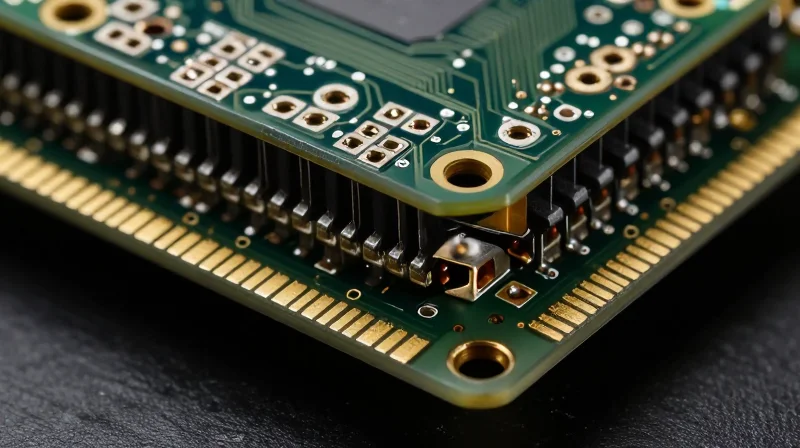
Critical Fabrication Hurdles in High-Density IVD Platforms
As IVD diagnostic hardware shifts toward increased miniaturization and multi-channel signal processing, the mechanical and electrical constraints on PCB fabrication have become significantly more stringent. Achieving reliable performance in these dense environments necessitates addressing three primary manufacturing bottlenecks: via-in-pad reliability, precision layer registration, and the management of high-aspect-ratio holes.
Manufacturing Challenge Comparison
| Manufacturing Process | Primary Challenge | Impact on IVD Reliability |
|---|---|---|
| Via-in-pad Plating | Void formation and uneven copper distribution | Potential intermittent signal loss and structural fatigue |
| Layer Registration | Registration tolerance drift in multi-layer stacks | Impedance mismatch and crosstalk between signal layers |
| High-Aspect-Ratio Drilling | Thermal stress and micro-cracking | Decreased lifespan in cyclic thermal diagnostic testing |
Frequently Asked Questions on PCB Manufacturing
- Why is via-in-pad plating critical for IVD sensors?
Via-in-pad technology allows for closer placement of surface-mount components, reducing signal path length and parasitic inductance, which is essential for capturing low-amplitude biological electrical signals. - How does layer-to-layer registration affect diagnostic sensitivity?
Precise registration ensures that high-speed signal lines remain equidistant from ground planes, maintaining a constant impedance profile that prevents signal reflection and minimizes electromagnetic interference. - What manufacturing standard should be adopted for high-reliability medical PCBs?
Manufacturers should prioritize IPC Class 3 standards, which dictate rigorous inspection criteria for internal layer registration, plating thickness uniformity, and solder joint integrity under thermal stress.
Ultimately, the transition toward advanced materials—such as low-Dk/low-Df laminates—must be mirrored by an equally sophisticated approach to fabrication. Without strictly controlled drilling and plating processes, the electrical benefits of these materials are negated by physical imperfections that degrade diagnostic signal quality.
Regulatory Compliance and Material Selection
Aligning Advanced PCB Materials with ISO 13485 Requirements
Transitioning to next-generation PCB materials—such as high-frequency laminates or advanced thermal management substrates—requires a rigorous approach to the ISO 13485 design control process. Manufacturers must demonstrate that the change in material composition does not inadvertently introduce biological risks or degrade the long-term reliability of signal processing chains. This involves proactive biocompatibility assessments, particularly for devices where PCBs reside in close proximity to fluidic pathways, and exhaustive verification that new materials maintain electrical stability across expected operating environments.
Medical-Grade Certification and Risk Management
| Material Innovation | Key Compliance Challenge | Regulatory Strategy |
|---|---|---|
| Low-Loss Laminates | Traceability of dielectric raw materials | Maintain certified Master File |
| Advanced Thermal Interfaces | Potential for outgassing and contamination | ISO 10993 cytotoxicity testing |
| Ultra-HD Interconnects | Failure modes in high-density structures | Expanded HALT/HASS validation |
Regulatory FAQs for PCB Technology Adoption
- Does changing the PCB base material constitute a 'significant change'?
Under most regulatory frameworks, if the material change alters the device's electrical safety, thermal profile, or biocompatibility, it is considered a significant change requiring a new regulatory submission or an internal change control impact analysis. - How is biocompatibility addressed for PCB components inside IVD fluidic enclosures?
Even if the PCB is not in direct contact with biological samples, the risk of volatile organic compound (VOC) emission or chemical migration necessitates ISO 10993 standard testing for all materials within the localized device environment. - What documentation is required from PCB fabricators?
Fabricators must provide a full Certificate of Conformance (CoC), documented evidence of REACH and RoHS compliance, and clear traceability back to the raw substrate manufacturer's batches.
Future-Proofing Your Next Diagnostic Product Design
Balancing Performance and Scalability
To future-proof IVD diagnostic hardware, engineering teams must move away from rigid, legacy-bound designs. The integration of high-frequency materials with modular signal processing architectures allows for a 'design-for-evolution' approach, where hardware components can be updated to support higher sensitivity assays without requiring a full system redesign.
| Strategy | Traditional Approach | Future-Proofing Approach |
|---|---|---|
| Signal Processing | Hard-coded ASIC integration | FPGA/SoC reconfigurable logic |
| Material Selection | Standard FR-4 | High-Tg/Low-Loss laminates |
| System Upgrades | Full PCB replacement | Modular daughter-board architecture |
Strategic Material Considerations
Selecting the right substrate is no longer just about dielectric constants; it is about managing thermal stability and signal integrity over the life cycle of a product. Investing in high-performance materials early in the prototyping phase mitigates the risks of signal degradation and ensures compliance with tightening EMI standards.
Frequently Asked Questions
- How do I justify the cost of advanced PCB laminates?
View advanced laminates as a risk-mitigation investment. The reduction in signal noise and improved reliability often pay for themselves by reducing re-certification cycles and field failures. - Is modular architecture better than monolithic design for IVD?
Modular designs significantly outperform monolithic designs in longevity, as they allow specific sensing modules to be upgraded to match newer microfluidic technologies without invalidating the entire system's regulatory filing. - Does material choice affect regulatory pathing?
Yes. Utilizing proven, medical-grade materials simplifies ISO 10993 and ISO 13485 compliance, as there is existing longitudinal data on how these materials behave under stress and sterilization.
The transition to point-of-care IVD success lies in the balance between signal fidelity and compact design. By shifting from legacy architectures to high-performance PCB material substrates, manufacturers can ensure their diagnostic tools meet the rigorous accuracy standards of tomorrow. Contact our engineering team today to audit your current PCB specifications and explore the latest innovations for your next IVD project.
