
In the world of In Vitro Diagnostics (IVD), the difference between a breakthrough measurement and a noise-contaminated false reading often lies in the architecture of the printed circuit board. As sensing hardware demands higher sensitivity, engineers must navigate the treacherous waters of signal integrity. This guide provides the authoritative DFM blueprint for maintaining absolute signal purity in high-precision, noise-sensitive IVD circuitry.
Understanding the IVD Signal Chain Challenges
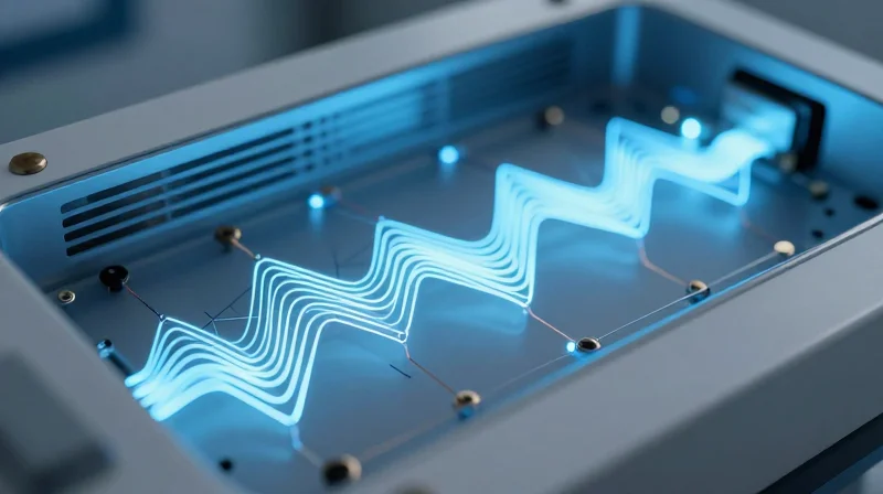
The Physics of Micro-Volt Sensitivity in IVD
In IVD instrumentation, the signal chain often originates from sensors detecting minute biological reactions—such as electrochemical potential changes or fluorescent photon counts—which typically operate at the micro-volt level. Because these signals are orders of magnitude smaller than typical digital noise floors, the PCB acts not just as a mechanical support, but as a sensitive transducer for ambient electromagnetic interference (EMI). Maintaining signal integrity necessitates a design strategy that prioritizes galvanic isolation and extreme low-noise front-end architecture.
Comparative Noise Sources in Diagnostic Environments
| Noise Source | Coupling Mechanism | Impact on IVD Signal |
|---|---|---|
| Switching Power Supplies | Conductive/Radiative | High-frequency ripples in sensor bias |
| Thermal Gradients | Seebeck Effect | Voltage offsets and signal drift |
| Radio Frequency (RF) | Radiative | Demodulation artifacts at DC |
| Mechanical Vibration | Piezoelectric Effect | Microphonic noise in high-impedance traces |
Common Signal Chain Challenges
- Why does trace length matter for micro-volt signals?
Longer traces act as antennas for ambient EMI. Reducing trace length minimizes the loop area, directly lowering the amount of coupled noise in high-impedance signal paths. - How does PCB material choice impact signal integrity?
Dielectric absorption and dissipation factors in standard FR-4 can introduce parasitic leakage currents, which are catastrophic when measuring signals in the low micro-volt regime. - What is the primary danger of mixed-signal layouts?
Digital return currents seeking the path of least impedance often infiltrate sensitive analog ground planes, causing ground bounce that masks diagnostic data.
Designers must recognize that in IVD applications, DFM is not merely about manufacturability, but about protecting the physical purity of the measurement. Failure to isolate the analog domain from the high-speed digital processing core often results in inconsistent diagnostic sensitivity and high failure rates in clinical environments.
Precision Stack-Up Geometry
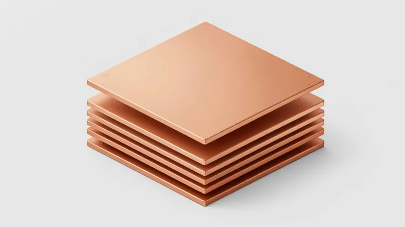
Symmetric Stack-Up Architecture
For high-precision IVD systems, a symmetric stack-up is not merely a design preference but a requirement for mechanical and electrical stability. By mirroring the copper distribution and dielectric thicknesses around the central core of the PCB, designers significantly reduce the risk of board warping during reflow, which can introduce micro-fractures in high-density interconnects. Electrically, symmetry ensures that signal layers are referenced to stable, equidistant ground planes, preventing common-mode noise generation.
| Parameter | Asymmetric Design | Symmetric Design |
|---|---|---|
| Mechanical Stress | High risk of bowing/warping | Minimized thermal stress |
| Return Current | Discontinuous impedance | Balanced and predictable |
| Signal Integrity | Susceptible to EMI | Optimized containment |
Strategic Ground Plane Placement
In micro-volt diagnostic circuits, the ground plane serves as the primary shield against ambient EMI and the secondary return path for high-frequency switching. To minimize crosstalk, each signal layer must be adjacent to an unbroken ground reference. By employing 'stripline' configurations where signal traces are sandwiched between two ground planes, designers achieve superior containment of electromagnetic fields, effectively isolating low-voltage analog paths from high-speed digital noise.
DFM Best Practices for Stack-Up Design
- Why must ground planes remain unbroken?
Splits or cutouts in the ground plane force return currents to take longer, indirect paths, creating large current loops that act as efficient antennas for noise radiation and susceptibility. - How does layer coupling affect crosstalk?
Decreasing the dielectric height between a signal trace and its reference plane concentrates the electromagnetic field tighter around the trace, significantly reducing the mutual inductance that drives crosstalk. - What is the role of prepreg in stack-up?
Using low-loss, stable-dielectric prepreg materials ensures that impedance remains consistent across varying temperatures, preventing signal timing jitter in high-precision measurement cycles.
Mastering Trace Impedance Control
The Imperative of Controlled Impedance in IVD Sensing
In high-precision in vitro diagnostic (IVD) systems, micro-volt level signals are highly susceptible to reflections caused by impedance discontinuities. Maintaining a consistent characteristic impedance (typically 50Ω for single-ended or 100Ω for differential pairs) is essential to minimize signal degradation, crosstalk, and EMI, ensuring the fidelity of the raw analog data captured at the sensor interface.
DFM Considerations for Fabrication Tolerances
Designing for manufacturability (DFM) in precision PCBs means accounting for the realities of the PCB fabrication process. Variations in dielectric constant (Dk), trace width, and copper thickness significantly impact impedance. Engineers must collaborate early with board houses to define realistic tolerance windows.
| Parameter | Typical Tolerance | Impact on Impedance |
|---|---|---|
| Trace Width | +/- 10% | Significant |
| Dielectric Thickness | +/- 5% | High |
| Dielectric Constant (Dk) | +/- 0.1 | Moderate |
| Copper Thickness | +/- 0.5 oz | Low to Moderate |
Practical Implementation Strategies
- How do I mitigate etch-back variability?
Request impedance coupons on the fabrication panel that match the trace geometry of your critical signal paths to verify that the etch factor is within specification. - What role does the dielectric play?
Select materials with stable Dk over temperature and frequency, such as high-performance FR-4 or PTFE-based laminates, to prevent impedance drift during diagnostic operation. - Should I use differential pair routing?
Yes, differential pairs are mandatory for sensitive analog signals; ensure tight coupling and symmetric routing to provide superior common-mode noise rejection.
By establishing a clear impedance control strategy and accounting for production variance during the design phase, IVD developers can significantly reduce noise floor issues, leading to more robust and reliable diagnostic outcomes.
Material Selection for High-Frequency Integrity
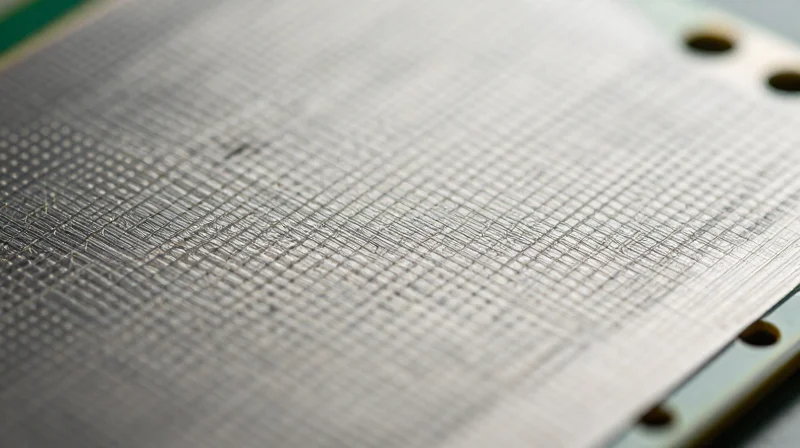
The Role of Dielectric Properties in IVD Performance
In low-signal IVD applications, the substrate material acts as both an insulator and a transmission medium. For frequencies ranging from baseband to high-speed digital interfaces, the dielectric constant (Dk) and dissipation factor (Df) directly influence signal velocity and attenuation. High-precision sensing requires materials that offer a stable Dk across temperature gradients, ensuring that impedance remains consistent throughout the device’s operational lifecycle.
Comparison of Common Substrate Materials
| Material Category | Typical Dk (1GHz) | Dissipation Factor (Df) | Application Suitability |
|---|---|---|---|
| Standard FR-4 | 4.5 | 0.020 | General digital logic only |
| High-Tg/Mid-Loss | 4.0 | 0.010 | Standard IVD control boards |
| Ultra-Low Loss (PTFE) | 2.2 - 3.0 | <0.002 | High-precision RF/Analog sensing |
Critical DFM Considerations for Substrate Selection
- Why should I prioritize glass weave effect?
Non-uniform glass fiber distribution can cause periodic variations in Dk, leading to skew in differential pairs. In precision IVD systems, specifying 'spread glass' or 'flat weave' fabrics is mandatory to ensure homogenous dielectric properties. - How does surface roughness impact signal integrity?
At higher frequencies, skin effect causes electrons to flow along the surface of the copper trace. High-profile copper foils create unnecessary resistance and phase delay; low-profile or VLP (Very Low Profile) copper should be utilized to minimize insertion loss. - What is the impact of moisture absorption?
IVD devices are often used in clinical environments with varying humidity. Substrates with high moisture absorption rates experience a shift in Dk, which can destabilize calibration parameters. Materials with low moisture absorption are preferred for consistent long-term performance.
Ultimately, the DFM process must involve early consultation with the PCB fabricator. Validating the specific material's thermal reliability and ensuring the pre-preg resin content is sufficient to fill internal gaps prevents signal discontinuities that are fatal to micro-volt sensing applications.
Minimizing Noise through Strategic Routing

Minimizing Noise through Strategic Routing
In IVD applications where micro-volt level sensing is common, signal integrity is often compromised by proximity-induced electromagnetic interference (EMI) and common-mode noise. Strategic routing requires a disciplined approach to differential pair topology, strict length matching protocols, and the physical segregation of sensitive analog front-end components from high-speed digital switching circuitry.
Differential Pair Precision and Length Matching
To ensure maximum common-mode rejection (CMRR), differential pairs must be routed with tightly coupled geometries to ensure that noise coupled into the traces appears as common-mode voltage. Length matching must account for both flight time differences and impedance discontinuities caused by via transitions.
| Routing Technique | Primary Benefit | DFM Constraint |
|---|---|---|
| Tight Coupling | Improved EMI Rejection | Maintain S/H ratio > 2:1 |
| Phase Matching | Reduced Jitter/Skew | Tolerance < 5 mil |
| Via Stitching | Impedance Stability | Keep-out zones > 3x hole diameter |
Critical Isolation Strategies
- How should analog and digital returns be managed?
Avoid splitting ground planes if possible; instead, use geographic partitioning to keep digital return currents away from the sensitive analog reference path. - Is Guard Tracing effective for high-precision signals?
Yes, but guard traces must be properly stitched to the ground plane with frequent vias to prevent them from acting as unintended slot antennas. - What is the role of 45-degree bends?
Use 45-degree bends or arc traces to minimize impedance discontinuities and reflections that occur at sharp 90-degree corners.
/* Example of differential pair clearance constraints */
Rule_Diff_Pair_Coupling {
  Min_Clearance: 0.15mm;
  Max_Length_Skew: 0.05mm;
  Backdrilling_Required: true;
}
Component Placement and Decoupling Best Practices
In high-precision In Vitro Diagnostic (IVD) systems, component placement is not merely a physical arrangement but a critical strategy for mitigating electromagnetic interference (EMI). Effective DFM practices for low-signal integrity require a spatial hierarchy that physically separates sensitive analog front-ends from noisy switching power converters and digital processing units.
Strategic Proximity and Isolation
Proximity management is the first line of defense against signal corruption. Sensitive sensors and ADCs should be shielded from high-dv/dt nodes. When placing components, prioritize the physical separation of ground planes—or the strategic use of star-grounding techniques—to prevent digital return currents from injecting noise into low-level analog signal paths.
| Component Category | Placement Rule | Isolation Requirement |
|---|---|---|
| Analog Front-End (AFE) | Near Input Connector | High Isolation from Digital |
| Switching Converters | Edge of Board | Shield from Sensitive Nodes |
| Clock/Oscillators | Near Load IC | Strict Ground Plane Reference |
PDN and Decoupling Best Practices
A robust Power Delivery Network (PDN) is essential to suppress transient noise at the source. Decoupling capacitors must be chosen for their self-resonant frequency (SRF) and placed to minimize loop inductance. For high-precision IVD applications, rely on multi-tier decoupling: bulk capacitors for low-frequency stability and 0201/0402 ceramic capacitors for high-frequency noise suppression.
- Why is capacitor proximity critical?
Minimizing the trace length between the power pin and the decoupling capacitor significantly reduces parasitic inductance, which is vital for providing instantaneous current during high-speed switching events. - Should I use via-in-pad for decoupling?
Yes, using via-in-pad or direct micro-via connection to the power plane is recommended to reduce loop area and inductance compared to traditional fan-out trace routing. - How do I select the right capacitor values?
Implement a Decoupling Pyramid strategy, utilizing a range of values (e.g., 10uF, 0.1uF, 100pF) to provide low impedance across a broad frequency spectrum.
EMI Mitigation and Shielding Strategies
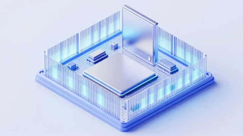
The Architecture of EMI Suppression
In high-precision IVD applications, electromagnetic interference (EMI) is not merely a compliance issue; it is a fundamental threat to the accuracy of micro-volt level analog sensors. Effective mitigation strategy relies on the principle of Faraday shielding and containment. Designers must treat the PCB as a modular ecosystem where high-frequency digital noise and high-gain analog amplification are spatially and galvanically isolated.
Implementation of Via Fencing and Stitching
Via fencing acts as a vertical boundary, effectively creating an electromagnetic 'wall' that prevents crosstalk between signal layers and prevents edge radiation. To be effective, the spacing between vias must be significantly smaller than the wavelength of the highest noise frequency—typically no greater than 1/10th of the wavelength.
| Technique | Primary Function | Design Rule Constraint |
|---|---|---|
| Ground Via Fencing | Lateral EMI Containment | Spacing < λ/20 for critical lines |
| Stitching Vias | PDN Impedance Reduction | Uniform grid across reference planes |
| Board-Level Shields (BLS) | External Field Rejection | Must provide low-inductance grounding |
FAQ: Shielding and Mitigation Best Practices
- When should physical board-level shields (BLS) be used over simple via fences?
Use physical BLS cans for high-gain analog front-ends (AFEs) that are susceptible to RF ingress from onboard wireless modules or high-speed processors where via fences provide insufficient attenuation. - How does stackup design affect EMI mitigation?
Always employ a stripline configuration with solid reference planes above and below the signal layer to minimize loop area, which is the primary source of EMI radiation. - Is there a penalty for over-using stitching vias?
While essential, excessive vias can introduce parasitic inductance and degrade thermal conductivity or structural integrity; place them strategically near signal transitions and high-frequency return paths.
DFM Verification and Simulation Workflows
The Shift-Left Approach to Signal Integrity
In high-precision diagnostics, the cost of a failed prototype is not merely financial; it represents significant delays in clinical regulatory pathways. Adopting a shift-left strategy—moving electromagnetic analysis and rule validation into the pre-layout phase—is the only way to ensure complex signal paths meet the stringent sensitivity requirements of IVD instruments.
Pre-Layout vs. Post-Layout Simulation
| Workflow Phase | Primary Goal | Common Toolset | Key DFM Impact |
|---|---|---|---|
| Pre-Layout | Stackup and Impedance Planning | 2D Field Solvers | Early detection of crosstalk risks |
| In-Layout | Constraint-Driven Routing | Interactive DRC Engines | Real-time length matching enforcement |
| Post-Layout | Parasitic Extraction | 3D EM Simulation | Validation of final EMI signatures |
Verification Workflows for High-Precision Designs
Modern PCB verification relies on the integration of automated Design Rule Checking (DRC) with physics-based simulation models. For diagnostic hardware, relying solely on standard DRC is insufficient because it cannot predict how high-frequency switching affects low-microvolt biological sensors.
- Why is 3D EM simulation essential for IVD sensors?
3D EM simulation captures the coupling effects of vias and connectors that 2D analytical tools miss, which is critical when tracking pA-level signals. - How do we bridge the gap between simulation and DFM?
By creating a 'single source of truth' where design constraints are exported directly from simulation results into the layout tool’s rule-set library. - What defines a robust verification check?
A robust workflow includes automated connectivity checks, impedance profile validation, and thermal reliability analysis to ensure environmental stressors don't drift the signal chain.
Achieving signal integrity in IVD systems is not just about adhering to rules—it is about creating a robust ecosystem where sensitive measurements thrive. By integrating these DFM strategies into your development pipeline, you can drastically reduce noise and ensure high-fidelity diagnostic performance. Contact our engineering team today to review your current board design and elevate your IVD product standards.
