
Transitioning from a functional prototype to a high-volume medical-grade flexible printed circuit assembly (FPCA) is a common hurdle for many engineering teams. While designs might work perfectly on the bench, they often fail under the rigors of mass production due to subtle violations in DFM principles. In this guide, we break down the engineering standards required to maintain precision in ultra-small flex circuits, ensuring your products remain reliable, scalable, and cost-effective.
Mastering Copper Thickness for Flexibility and Reliability

The Mechanical Imperative of Thin Copper
In medical device design, particularly for dynamic applications like catheters or endoscopes, conductor fatigue is the primary failure mode. Thinner copper foils—specifically 1/3 oz (12µm) and 1/2 oz (18µm)—are essential because they sit closer to the neutral axis of the flexible stack-up. This reduced cross-section minimizes the strain exerted on the copper during repetitive bending, effectively preventing work-hardening and premature fracturing that would occur with thicker 1 oz or 2 oz materials.
Copper Thickness Comparison for Flex Performance
| Copper Weight | Nominal Thickness | Flexibility Profile | Best Use Case |
|---|---|---|---|
| 1/3 oz | 12µm | Excellent | High-density, multi-layer dynamic flexing |
| 1/2 oz | 18µm | Good | Standard dynamic and semi-rigid medical circuits |
| 1 oz | 35µm | Poor | Static applications or high-current power paths |
DFM Guidelines for Ultra-Small Assemblies
- Why is 1/3 oz copper preferred for ultra-small medical designs?
Beyond mechanical flexibility, 1/3 oz copper allows for finer trace widths and tighter pitch spacing, which is critical for miniaturizing interconnects in small-diameter medical probes. - How does copper grain structure impact reliability?
Always specify Rolled Annealed (RA) copper over Electro-Deposited (ED) copper. The elongated grain structure of RA copper offers superior ductility and resists micro-crack propagation under repeated stress. - Are there electrical trade-offs to using thinner copper?
Thinner copper increases DC resistance. Engineers must calculate thermal rise and voltage drop carefully, potentially widening traces to compensate for the reduced cross-sectional area.
Optimizing Trace-to-Space Ratios in Micro-Flex Layouts
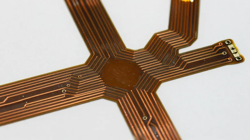
The Etching Limit Constraint
In ultra-small medical assemblies, the primary constraint on trace-to-space density is the chemical etching process. As copper foils become thinner to allow for greater flexibility, the aspect ratio of the etch—often referred to as the 'etch factor'—becomes critical. Designers must account for undercut, where the chemical etchant dissolves copper beneath the photoresist, potentially reducing the trace cross-section and degrading signal performance if tolerances are too aggressive.
Manufacturing Tolerance Matrix
| Copper Weight | Min Trace Width | Min Trace Space | Risk Profile |
|---|---|---|---|
| 1/3 oz (12µm) | 25µm | 25µm | High: Etch factor sensitivity |
| 1/2 oz (18µm) | 50µm | 50µm | Moderate: Reliable production |
| 1 oz (35µm) | 100µm | 100µm | Low: Standard high-yield |
Maintaining Signal Integrity at Scale
Shrinking trace widths significantly increases DC resistance and can lead to impedance mismatches in high-speed medical sensor data. To maintain signal integrity while shrinking footprints, designers should prioritize controlled-impedance routing through wider, shorter traces when possible, and transition to microvias for interlayer connectivity to minimize the overall circuit area without narrowing primary traces.
- How does trace width affect mechanical reliability?
Narrower traces are less susceptible to fracture during bending, but increased resistance can lead to thermal micro-stress at contact points. - Why is the etch factor critical for ultra-small designs?
An improper etch factor results in non-rectangular trace profiles, causing impedance variations that are magnified as physical dimensions decrease. - What is the recommended design strategy for high-density flex?
Utilize 'staggered' trace routing to maximize space between conductors, reducing the risk of bridging during the etching process.
Coverlay Registration: Strategies for Alignment Accuracy
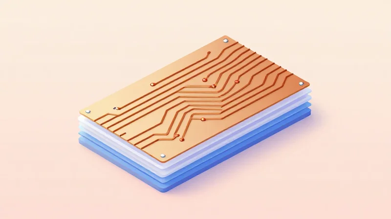
Managing Coverlay Registration and Alignment
In ultra-small medical flexible printed circuit assemblies (FPCAs), coverlay registration is a critical DFM challenge. Because polyimide coverlays are dimensionally unstable, thermal expansion and moisture absorption can lead to misalignment during the lamination process. Engineers must implement generous 'coverlay access' openings and apply scaling factors to compensate for material stretch to prevent the coverlay from encroaching on pads, which causes shorts or insufficient solder fillets.
Strategies for Mitigating Registration Errors
- Enlarged Access Openings
Increase coverlay opening sizes by at least 0.1mm to 0.2mm relative to the copper pad size. This buffer accounts for standard lamination drift while maintaining adequate insulation. - Webbing Preservation
Ensure adequate 'web' width between adjacent pads. Reducing coverlay openings too aggressively can lead to thin bridges of polyimide that tear during assembly, creating debris or reliability hazards. - Scaling and Compensation
Consult with your fabricator to determine the specific X and Y scaling factors needed to compensate for polyimide expansion during high-temperature pressing.
| Parameter | Standard Tolerance | High-Precision (Medical) |
|---|---|---|
| Registration | +/- 0.25mm | +/- 0.075mm |
| Coverlay Opening | Pad Size + 0.15mm | Pad Size + 0.05mm |
| Web Width | 0.15mm | 0.075mm |
Design Best Practices for Solder Masking
For the highest density designs, traditional polyimide coverlay may be too coarse. Consider using liquid photoimageable (LPI) coverlay as a substitute for extremely small medical circuits where registration requirements exceed the mechanical limits of sheet-based polyimide. LPI offers precision comparable to standard solder masks, providing tighter alignment for fine-pitch surface mount components and micro-vias.
Bend Radius and Mechanical Stress Mitigation

Engineering for Durability: The Neutral Axis Principle
The fundamental principle of robust flexible circuit design is positioning copper conductors within the 'neutral axis' of the stackup. When a circuit is bent, the outer layers experience tensile stress while inner layers experience compressive stress; the neutral axis is the geometric plane where these stresses cancel out. For ultra-small medical devices, failure to balance this stackup often results in work-hardening, micro-fracturing, or complete trace delamination during repetitive motion.
Best Practices for Trace Routing in Bend Zones
- Staggered Trace Patterns
Avoid stacking traces directly on top of each other across bend lines. Staggering traces prevents a 'stiff' region that resists bending and prevents local stress concentrations. - I-Beam vs. Flat Conductor Routing
Always prefer flat, wide trace routing over I-beam construction, as I-beam configurations create stress risers at the sharp corners of the trace cross-section. - Trace Orientation
Route traces perpendicular to the bend line whenever possible to minimize the length of the conductor exposed to mechanical strain. Avoid diagonal routing through high-flex areas. - Radius Ratios
Maintain a minimum bend radius-to-thickness ratio of at least 10:1 for static applications and 20:1 to 50:1 for dynamic flexing in medical instruments.
| Design Feature | High Stress (Avoid) | Low Stress (Recommended) |
|---|---|---|
| Trace Stacking | Aligned directly over each other | Staggered/offset patterns |
| Copper Profile | Thick, high-profile copper | Rolled-annealed (RA) thin copper |
| Bend Geometry | Sharp 90-degree angles | Large radius arcs or rounded curves |
| Trace Entry | Perpendicular entry to pads | Teardrop or fillet connections |
Critical DFM Rules for Medical Reliability
To ensure long-term performance, incorporate 'teardropping' at every junction where a trace enters a pad. This spreads the mechanical load away from the brittle interface of the pad and trace. Additionally, use curved traces instead of angular ones; sharp corners act as stress concentrators that initiate cracks under cyclic loading. For multi-layer designs, ensure that the substrate thicknesses are symmetric relative to the central copper layer to maintain the neutral axis effectively.
Material Selection: Adhesive vs. Adhesiveless Systems
Material Selection: Adhesive vs. Adhesiveless Systems
For high-reliability medical electronics, the interface between the copper foil and the polyimide dielectric is a primary point of failure. Adhesive-based laminates utilize epoxy or acrylic bonding layers, which introduce CTE (Coefficient of Thermal Expansion) mismatches and potential outgassing issues. In contrast, adhesiveless constructions—where copper is deposited directly onto the polyimide—provide a thinner, more flexible, and thermally stable profile essential for miniaturized medical sensors and implants.
| Feature | Adhesive-Based | Adhesiveless |
|---|---|---|
| Total Thickness | Thicker (adds bonding layer) | Thinner (optimal for micro-flex) |
| Dimensional Stability | Lower (adhesive can shift) | Higher (integral bond) |
| Thermal Stability | Moderate (Tg limits) | High (excellent heat resistance) |
| Signal Integrity | Variable dielectric constant | Superior/Consistent |
Key DFM Considerations for Adhesiveless Systems
Adhesiveless systems offer superior performance, but they require stringent manufacturing controls due to the absence of the compliant adhesive layer that traditionally absorbs internal mechanical stress during bending. When designing for ultra-small medical devices, consider the following performance impacts.
- Why is adhesiveless preferred for high-density medical FPCAs?
The absence of a middle bonding layer allows for a significantly lower profile and improved flexibility. This is crucial for tight-tolerance, multi-layer designs where every micron counts toward minimizing the overall bend radius. - How does material choice affect trace fracturing?
Adhesive layers are inherently soft and can act as a cushion. Adhesiveless systems provide a more rigid interface; therefore, copper traces must be designed with greater attention to the neutral axis to prevent stress fractures during repeated flexing. - Does material choice impact chemical resistance?
Yes, standard adhesives are often porous and prone to moisture absorption or degradation when exposed to medical-grade cleaning agents or autoclave sterilization processes. Adhesiveless polyimide is far more inert and reliable in these harsh environments.
Ultimately, for medical applications involving miniaturized interconnects or complex dynamic flexing, specifying adhesiveless materials is an industry-standard recommendation to ensure long-term device performance and compliance with rigorous regulatory safety standards.
Pad and Via Design for High-Density Interconnects
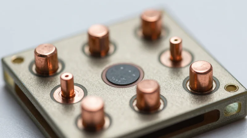
Pad Geometry and Copper Retention Strategies
In ultra-small medical flexible circuits, pad peeling is a primary failure mode caused by repeated thermal cycling and mechanical flexing. To prevent copper lifting, designers must prioritize increased surface area contact and improved mechanical anchoring of SMT pads.
- Extended Pad Anchors
Utilize 'anchor spurs' or extended copper tabs that extend beneath the coverlay opening. This provides a physical lock between the pad and the dielectric substrate. - Radiused Corners
Avoid sharp 90-degree corners on SMT pads to minimize stress concentration points that typically trigger crack propagation during thermal expansion. - Coverlay Capture
Ensure the coverlay opening is smaller than the pad geometry to create a 'solder mask defined-like' effect on flex, anchoring the pad edges securely.
Via-in-Pad (VIP) Configuration and Reliability
While via-in-pad (VIP) is essential for high-density medical designs, it introduces risks related to solder wicking and plating stress. For flexible substrates, plating ductility is the most critical factor.
| Feature | Standard Flex Rule | Medical-Grade Recommendation |
|---|---|---|
| Via Plating Thickness | 20-25 micron | 30+ micron (for ductility) |
| Via-in-Pad Fill | Non-conductive epoxy | Copper-filled with cap plating |
| Teardropping | Optional | Mandatory on all via-to-trace junctions |
Teardropping and Interconnect Reinforcement
Teardropping is not merely an aesthetic choice in medical flex design; it is a critical requirement to increase the cross-sectional area of the via-to-trace junction. This design feature absorbs mechanical stress that would otherwise cause trace necking or fracturing at the drill breakout point.
- Why is teardropping critical for high-density flex?
It significantly reduces the 'stress riser' effect at the transition point between the rigid hole wall and the flexible trace, preventing delamination. - How to handle via-in-pad solder wicking?
Always employ laser-drilled, copper-filled microvias with flat plated-over caps to create a reliable, planar landing zone for SMT components.
Streamlining the Prototype-to-Production Transition
The Prototype-to-Production Checklist
Moving from a functional prototype to a scalable medical-grade product demands a transition from manual verification to automated DFM rigor. A successful handover requires addressing component tolerances, stack-up validation, and manufacturing documentation that leaves no room for ambiguous interpretation by the fabrication house.
| Parameter | Prototype Goal | Production Goal |
|---|---|---|
| Data Format | Visual/Manual | Automated ODB++ |
| Tolerance | Functionality | Process Capability (Cpk) |
| BOM | Availability | Life Cycle/Compliance |
Essential DFM Validation Steps
- Automated DFM Analysis
Run automated DFM checks for annular ring violations, copper-to-edge clearances, and drill-to-copper alignment before finalizing design data. - Stack-up Verification
Confirm the final polyimide thickness and adhesive types match the thermal expansion requirements of the specific sterilization cycle used in medical settings. - Panelization Strategy
Collaborate with the assembly partner to design a panel array that optimizes material utilization while preventing stress points on the flex circuits.
Frequently Asked Questions
- When should I involve the CM in the DFM process?
Contract Manufacturers should be engaged during the design-for-assembly (DFA) phase to ensure the layout accommodates the specific pick-and-place equipment. - Why is Gerber data insufficient for medical FPCAs?
Gerber files lack the intelligent connectivity data required for high-density interconnects, which increases the risk of misinterpretation; ODB++ or IPC-2581 are industry standards for robust production.
Achieving successful yields in medical-grade flex PCB manufacturing is not just about avoiding errors; it is about intentional design for the factory floor. By applying these DFM best practices, you minimize the risk of costly re-spins and ensure your medical devices perform flawlessly under the most demanding conditions. Ready to scale your next medical project? Contact our engineering team today for a comprehensive DFM audit of your current design files.
