
High-current motor controllers demand more than standard FR4 performance. In the e-bike industry, thermal failure is the leading cause of field returns. By shifting to aluminum-backed printed circuit boards (MCPCBs), engineers can achieve superior heat dissipation, but only if the layout follows specific design-for-manufacturing (DFM) rules. This guide explores how to balance electrical conductivity with thermal efficiency to ensure your controller survives the toughest terrain.
Understanding the Anatomy of an Aluminum-Backed PCB
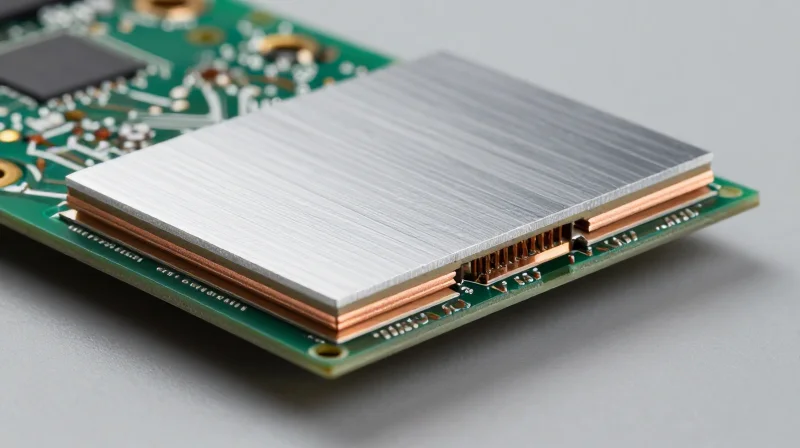
An aluminum-backed PCB, commonly referred to as a Metal Core PCB (MCPCB), acts as a high-performance thermal management solution by replacing the traditional epoxy-glass substrate with a metal base. In the context of e-bike motor controllers, this structure is vital for dissipating heat generated by high-power MOSFETs and power-switching components.
The Tri-Layer Structural Composition
The efficacy of an aluminum PCB relies on the precise synergy between its three fundamental layers. Understanding these layers is the first step in applying advanced DFM rules for high-current applications.
| Layer | Material | Primary Function |
|---|---|---|
| Circuit Layer | Copper Foil | Electrical signal and power routing |
| Dielectric Layer | Thermally Conductive Polymer | Electrical insulation while facilitating heat transfer |
| Base Layer | Aluminum Alloy | Mechanical support and heat dissipation sink |
Critical Performance Considerations
- What is the primary role of the dielectric layer?
The dielectric layer is the 'bottleneck' of thermal resistance. It must provide high dielectric strength to prevent shorting while remaining thin and conductive enough to channel heat from copper traces to the aluminum base. - How does the aluminum base affect PCB layout?
The aluminum base is conductive; therefore, no traces can be placed on the bottom side of the dielectric, and specific design rules regarding mounting holes and edge milling must be followed to avoid accidental grounding. - Why is copper foil thickness critical for e-bike controllers?
E-bike controllers manage high amperage, which generates significant resistive heating. Heavier copper foils (e.g., 2oz or 3oz) are required to reduce trace resistance, which in turn reduces the thermal burden placed on the dielectric layer.
Dielectric Layer Thickness and Breakdown Voltage
The Thermal-Dielectric Trade-off
In aluminum-backed PCBs (MCPCBs), the dielectric layer is the primary bottleneck for thermal resistance. While thinner layers significantly improve heat transfer from the power MOSFETs to the aluminum base, they inversely reduce the dielectric withstand voltage (DWV). For high-current E-bike controllers, designers must select a thickness that satisfies peak voltage transients while preventing premature thermal saturation.
Comparative Analysis of Dielectric Specifications
| Thickness (μm) | Thermal Conductivity (W/mK) | Dielectric Strength (kV) | Recommended Application |
|---|---|---|---|
| 50 | 2.0 - 3.0 | 2.5 - 3.0 | Low-voltage/High-thermal density |
| 75 | 1.5 - 2.2 | 3.0 - 4.5 | Standard E-bike (36V-48V) |
| 100+ | 1.0 - 1.5 | 5.0+ | High-voltage (72V+) industrial |
Critical Design Guidelines
- How does voltage rating influence thickness?
The dielectric must withstand peak bus voltage plus a safety margin for switching transients. For 48V systems, a minimum of 75μm is standard to ensure reliability under thermal stress. - Why is filler particle size important?
Modern high-thermal-conductivity dielectrics use ceramic fillers. If the dielectric layer is too thin, filler particles can create microscopic bridge paths that degrade insulation resistance over time. - What is the impact of thermal cycling?
E-bike controllers face extreme thermal cycling. Thicker dielectrics are more robust against mechanical delamination but require more aggressive heat sinking to compensate for the lower thermal conductivity.
To ensure long-term reliability, designers should always perform a partial discharge test on the final stack-up. Selecting a dielectric with higher thermal conductivity rather than simply thinning the layer is the preferred DFM strategy to achieve the target performance-to-safety ratio.
Advanced Trace Geometry for High-Current Density
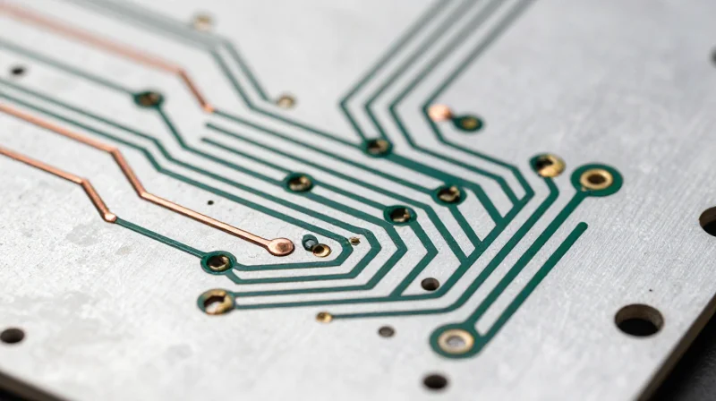
Optimizing Trace Width and Copper Weight for Aluminum Substrates
In high-current e-bike controllers, the trace geometry on aluminum substrates must be calculated differently than on standard FR4. Because the aluminum base acts as an aggressive heat sink, copper traces on MCPCBs often exhibit higher current-carrying capacity due to improved heat extraction. However, excessive trace width increases parasitic capacitance and board real estate, while overly thin copper leads to excessive I²R losses and voltage drops that degrade motor performance.
Design Guidelines for Trace Performance
| Copper Weight | Current Capacity (Steady State) | Recommended Application |
|---|---|---|
| 1 oz (35µm) | Low (up to 10A) | Control Logic and Signal Traces |
| 2 oz (70µm) | Moderate (10A - 30A) | Low-Power MOSFET Gate Drives |
| 3 oz+ (105µm+) | High (30A - 100A+) | Main Phase Power Lines |
For main motor phase lines, we recommend a minimum copper weight of 3 oz to minimize DC resistance. When laying out these traces, ensure that the traces are positioned directly over thermally conductive regions to maximize heat transfer to the aluminum base, thereby preventing localized hotspots at interconnect points.
Frequently Asked Questions on Trace Layout
- Does the aluminum base allow for thinner traces?
Yes, to an extent. The superior thermal conductivity of the aluminum base allows for a slightly lower cross-sectional area compared to FR4, but thermal impedance of the dielectric layer remains the limiting factor. - How does trace length impact voltage drop in phase lines?
Phase lines must be as short and direct as possible. Long, narrow traces in high-current paths increase inductance and resistance, which directly causes torque ripple and increased heat in the controller's power stage. - Is internal copper necessary?
Most aluminum PCBs are single-layer. If multi-layer designs are required, ensure the prepreg between layers is high-thermal-conductivity material to prevent thermal trapping.
Thermal Via Strategy and Heat Spreading
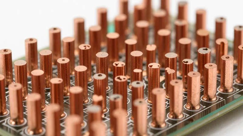
Thermal Via Strategy and Heat Spreading
In aluminum PCB architectures, thermal vias act as critical conductive pillars that bypass the inherently high thermal resistance of the dielectric layer. To maximize heat flux from high-power MOSFETs, designers must implement dense via arrays directly beneath the component thermal pads, ensuring these vias are filled and capped to maintain a planar surface for component mounting while creating a direct copper-to-dielectric-to-base path.
Optimizing Copper Pour for Heat Spreading
Copper pour acts as a secondary heat sink, effectively increasing the surface area for lateral heat distribution before vertical transfer to the aluminum base. For motor controllers, prioritize thick copper (2oz or 3oz) and ensure that large pours are not isolated, but rather integrated into the thermal pad architecture using wide thermal relief spokes or solid connections to minimize thermal impedance.
| Parameter | Recommended Practice | Benefit |
|---|---|---|
| Via Pitch | 0.8mm to 1.2mm | Balanced thermal conductivity vs. manufacturing yield |
| Via Plating | 25-30 micron minimum | Increased cross-sectional area for heat flow |
| Copper Weight | 2oz or higher | Enhanced lateral heat spreading |
- Why must vias be filled and capped?
Filling and capping prevents solder wicking during reflow, which otherwise creates voids under the component and significantly reduces thermal contact efficiency. - How does the dielectric layer influence via placement?
The thinner the dielectric, the more efficiently heat transfers, but high-current controllers often require thicker layers for isolation; therefore, increased via count is necessary to compensate for higher thermal resistance. - Is there a limit to thermal via density?
Yes; excessive via density can weaken the structural integrity of the copper foil and impede chemical etching processes, potentially leading to delamination.
Edge Clearance and Mechanical Constraints
Edge Clearance and Dielectric Integrity
When designing on aluminum substrates, the board edge is a primary failure point for high-voltage arcing. Because the aluminum base acts as a reference ground plane, any conductive feature—such as copper traces or planes—brought too close to the mechanical edge risks a catastrophic short circuit through the dielectric layer or across the board surface.
For e-bike motor controllers operating at 48V to 72V or higher, a standard clearance of 1.0mm from the copper edge to the board profile is often insufficient. Engineers must enforce a 'keep-out' zone that accounts for the precision of the mechanical cutting process (typically V-score or router bit tolerance) and the creepage requirements mandated by safety standards such as UL 62368-1.
Comparative Clearance Standards
| Voltage Rating (DC) | Minimum Edge Clearance | Considerations |
|---|---|---|
| 24V - 36V | 0.8mm | Standard safety margins |
| 48V - 60V | 1.2mm | Increased risk of dust accumulation |
| 72V+ | 1.5mm - 2.0mm | Creepage and humidity resistance |
Mechanical Constraints and Stress Management
Aluminum substrates exhibit different mechanical stress profiles compared to FR4. The rigidity of the metal base prevents flexing, which protects the solder joints of high-mass components like large electrolytic capacitors or power inductors; however, this lack of compliance means that thermal expansion stresses are focused entirely on the components themselves rather than the board.
- Why should high-mass components be placed away from the edges?
Edges are subject to vibration and potential mechanical shock during e-bike operation; locating heavy components too close to the periphery can lead to solder joint fatigue due to limited substrate vibration damping. - How does the routing process impact edge clearances?
Mechanical routing leaves burrs or micro-tears in the dielectric. A larger clearance provides a necessary buffer zone to ensure these conductive burrs do not bridge the gap to the aluminum core. - What role does solder mask play at the edge?
Solder mask should be omitted from the edge periphery to prevent cracking during the routing process, which could create paths for moisture ingress, compromising long-term dielectric performance.
Solder Mask and Surface Finish Considerations
In high-current motor controllers, the selection of solder mask and surface finish is not merely aesthetic; it is a critical thermal management decision. Aluminum PCBs utilize a thermally conductive dielectric layer that creates a unique Coefficient of Thermal Expansion (CTE) mismatch between the metal base, the dielectric, and the copper circuit layer. Choosing high-glass-transition temperature (Tg) solder masks and robust surface finishes is vital to prevent layer delamination and oxidation during peak thermal cycling.
Solder Mask Performance in High-Power Applications
Standard solder masks may degrade or become brittle under the intense heat generated by high-torque motor operation. For aluminum substrates, specify thermally conductive solder masks that offer superior adhesion properties and higher heat resistance. It is critical to ensure the mask is compatible with the specific dielectric layer to prevent localized peeling, which can compromise the creepage and clearance distances required for high-voltage phase lines.
Surface Finish Reliability Analysis
| Surface Finish | Thermal Durability | Suitability for High-Current | Recommendation |
|---|---|---|---|
| ENIG | Moderate | High (Flat surface) | Recommended for fine pitch components |
| HASL (Lead-Free) | High | Low (Uneven thickness) | Avoid due to uneven copper surface |
| Immersion Silver | Good | High | Ideal for cost-effective conductivity |
| ENEPIG | Excellent | Very High | Best for long-term thermal cycling |
Common DFM Considerations and FAQs
- Does the surface finish affect thermal transfer?
While the finish itself is thin, the flatness of the finish (like ENIG or ENEPIG) ensures better thermal interface material (TIM) contact, which significantly improves heat dissipation into the aluminum base. - Why is HASL discouraged for aluminum PCBs?
HASL creates an uneven surface that can cause issues with component alignment and, more importantly, creates unpredictable thermal paths that can lead to hot spots under high-current MOSFETs. - How does CTE mismatch affect solder mask longevity?
Rapid expansion of the aluminum base vs. the copper trace during heavy acceleration cycles puts stress on the solder mask; using a flexible, high-Tg mask helps accommodate these mechanical micro-stresses without cracking.
Avoiding Common Assembly-Related Bottlenecks
Mitigating Assembly-Level Bottlenecks in Aluminum PCBs
Aluminum PCBs present unique challenges during assembly compared to standard FR-4 substrates, primarily due to high thermal conductivity and the coefficient of thermal expansion (CTE) mismatch between the metal base, the dielectric layer, and the copper circuit. Failure to account for these dynamics often results in delamination, solder joint fatigue, or poor heat dissipation.
Critical Assembly Risks and Mitigation Strategies
| Risk Factor | Primary Impact | Mitigation Strategy |
|---|---|---|
| CTE Mismatch | Delamination/Cracking | Optimize ramp rates in reflow profiles. |
| Surface Non-planarity | Inconsistent Heat Sinking | Apply thermally conductive interface materials. |
| High Thermal Mass | Cold Solder Joints | Increase soak time during reflow. |
Frequently Asked Assembly Questions
- How does the aluminum base impact reflow oven settings?
The metal core acts as an aggressive heat sink, effectively drawing thermal energy away from the solder joints. You must calibrate your reflow profile with a higher soak temperature and longer duration to ensure uniform solder melting across the high-current components. - Can I prevent delamination during high-temperature assembly?
Avoid rapid temperature spikes. Use a multi-stage preheating process to allow the aluminum base and dielectric layers to expand at a controlled rate, reducing localized stress that leads to delamination. - What is the best way to ensure thermal contact with the controller chassis?
Surface unevenness in the aluminum base can create air gaps. Ensure the assembly process specifies high-pressure clamping during final integration and utilizes high-performance thermal interface materials (TIM) to fill microscopic voids.
Reflow Profile Optimization Guidelines
Set Preheat: 150-180°C (Extended Soak: 90-120s)
Time Above Liquidus: 60-90s
Cooling Rate: < 3°C/s (Avoid thermal shock)
Max Peak Temp: 245°C (Ensure thermal mass compensation)
Validation and Thermal Simulation Benchmarks
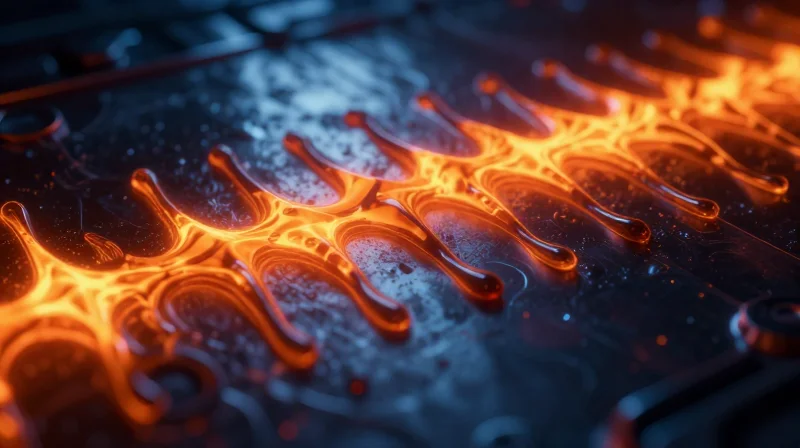
The Necessity of Pre-Fabrication Thermal Simulation
Aluminum substrates exhibit significantly different thermal dynamics compared to standard FR-4 due to the high thermal conductivity of the metal base. Before committing to fabrication, designers must employ finite element analysis (FEA) to predict heat flow under peak motor current loads. By modeling the thermal resistance path from MOSFET junctions to the aluminum heat sink interface, teams can identify hotspots that would otherwise lead to premature solder joint failure or dielectric breakdown.
Core Benchmarking Metrics
| Parameter | Target/Benchmark | Justification |
|---|---|---|
| Max Junction Temp (Tj) | < 125°C | Prevent MOSFET degradation |
| Dielectric Temp Rise | < 30°C over base | Protect insulation integrity |
| Solder Joint Fatigue | Low Stress Index | Mitigate CTE mismatch impact |
Validation Workflow for E-Bike Controllers
- How do you validate simulation accuracy?
Perform correlation testing using infrared thermography on physical prototypes under actual phase current conditions to confirm simulation offsets. - What simulation boundary conditions are mandatory?
You must accurately define the Thermal Interface Material (TIM) properties, convective cooling coefficients, and the ambient environment of the controller housing. - When is a redesign required during the simulation phase?
A redesign is mandatory if localized power densities exceed the heat-spreading capacity of the aluminum core, typically indicated by non-linear temperature spikes at current-carrying vias.
Mastering aluminum PCB design is the difference between a reliable e-bike motor controller and a costly warranty claim. By strictly adhering to these DFM principles—focusing on dielectric performance and optimized thermal pathways—you can design hardware that thrives under load. Ready to refine your next design? Download our comprehensive PCB Design Checklist or contact our engineering team to review your project files today.
