
In the world of medical electronics, a printed circuit board is more than a carrier for components; it is a critical safety system. Designing PCBs for AED defibrillators requires balancing extreme high-voltage energy storage with the strict reliability mandated by human-life applications. If your design fails, the stakes are not just hardware failure, but life and death. This guide explores the engineering rigor required to survive the scrutiny of IEC 60601 standards.
Understanding IEC 60601-1 Medical Device Standards
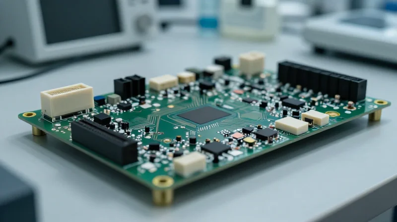
The Critical Role of IEC 60601-1 in High-Voltage AED Design
For designers of Automated External Defibrillators (AEDs), IEC 60601-1 serves as the global benchmark for safety. Because these devices involve high-voltage capacitors and patient contact, the printed circuit board (PCB) design must mitigate risks related to electric shock, fire, and mechanical hazards. Compliance is not merely a legal requirement for market entry; it is a fundamental architecture mandate that dictates trace spacing, component selection, and isolation strategies to ensure patient and operator safety during a cardiac emergency.
Key Safety Parameters for AED PCBs
| Requirement | PCB Design Implication | Safety Goal |
|---|---|---|
| Creepage/Clearance | Increased spacing for high-voltage traces | Prevention of arcing and short-circuits |
| Isolation (MOPP) | Use of reinforced opto-isolators/transformers | Patient protection from line voltage |
| Dielectric Strength | Use of high-CTI PCB materials | Insulation breakdown prevention |
Common Compliance Questions
- How do I determine isolation requirements for a defibrillator PCB?
You must classify the circuit based on Means of Patient Protection (MOPP) and Means of Operator Protection (MOOP). Defibrillator output circuits require 2xMOPP to ensure that a single component failure does not expose the patient to hazardous voltages. - Why is Comparative Tracking Index (CTI) critical for AED PCBs?
High-voltage boards are susceptible to surface tracking, where carbon paths form between traces. High CTI-rated laminates resist this degradation, ensuring the board maintains insulation integrity over the expected lifetime of the device. - Does IEC 60601-1 cover software reliability in PCB control circuits?
While IEC 60601-1 focuses on electrical safety, it references IEC 62304 for software lifecycle. The PCB design must provide hardware support for watchdog timers and safe state monitors to satisfy these regulatory expectations.
Mastering Creepage and Clearance for High Voltage
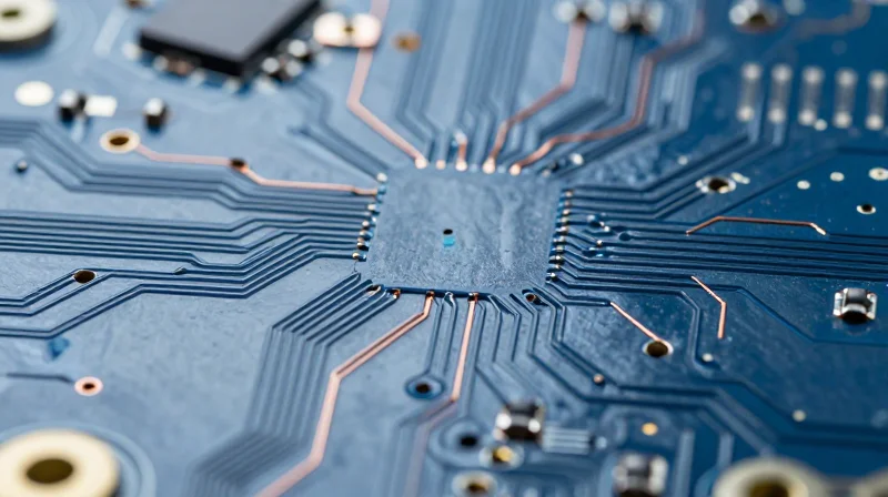
For AED defibrillator circuits, where high-energy capacitor discharge is required, mastering electrical isolation is not merely a design preference but a fundamental safety requirement. Designers must implement robust spacing protocols that account for peak transient voltages, surface contamination, and atmospheric pressure changes that can induce dielectric breakdown.
Calculating Spacing for High-Voltage Rails
The primary objective is preventing ionization of the air or carbon tracking across insulating materials. Clearance (the shortest path through air) and creepage (the shortest path along the surface of an insulator) must be determined based on the insulation type and expected pollution degree within the device housing.
| Parameter | Definition | Primary Failure Mode |
|---|---|---|
| Clearance | Shortest distance in air | Arcing/Ionization |
| Creepage | Shortest path along surface | Carbon Tracking/Pollution |
DFM Strategies for Arcing Prevention
- Slotting and Milling
Increase effective creepage paths by milling slots in the PCB substrate between high-voltage nodes, effectively breaking the conductive surface path. - Conformal Coating
Apply high-dielectric strength conformal coatings to reduce pollution degree requirements, though this should be a secondary mitigation rather than a substitute for physical spacing. - Keep-out Zones
Implement strict keep-out zones beneath high-voltage traces to prevent crosstalk and coupling into sensitive low-voltage control circuitry.
Common Implementation Questions
- How does atmospheric pressure affect clearance?
Lower pressure reduces the dielectric strength of air, meaning AEDs intended for use in high-altitude environments require significantly increased clearance distances to prevent arcing. - Why is CTI (Comparative Tracking Index) important?
Selecting PCB materials with a high CTI rating is essential, as these materials are more resistant to conductive track formation when subjected to electrical stress in the presence of moisture or impurities.
Material Selection: Choosing the Right Substrate
The Critical Role of Comparative Tracking Index (CTI)
In defibrillator circuitry, the substrate acts as a primary insulator against high-voltage gradients. The Comparative Tracking Index (CTI) is the most vital metric here; it quantifies a material's resistance to surface tracking—the formation of conductive paths through carbonization caused by electrical stress and moisture. For high-voltage AED applications, standard FR-4 (often CTI < 175V) is insufficient and poses a significant risk of catastrophic board failure over time.
Material Comparison for High-Voltage Applications
| Material Type | Typical CTI Rating | HV Performance | Application Suitability |
|---|---|---|---|
| Standard FR-4 | 150V - 175V | Low | Not recommended for HV areas |
| High-CTI FR-4 | 600V+ | High | Standard for AED main boards |
| Polyimide | 500V+ | Very High | High-temp/Flex environments |
| Ceramic-filled Laminates | 600V+ | Excellent | High-power switching zones |
Key Considerations for Substrate Selection
- Why is CTI 600V considered the industry benchmark?
A CTI of 600V places the material in the highest performance category (Material Group I), allowing for smaller creepage distances under IEC 60601-1 standards without increasing the risk of arcing. - How does moisture impact material selection?
AEDs are often used in varied environmental conditions. High-CTI materials resist the ionic contamination that leads to dendritic growth, ensuring the PCB remains stable even in high-humidity emergency scenarios. - What is the impact of thermal cycles on dielectrics?
The rapid discharge of high-voltage capacitors generates localized heat. Choosing a substrate with a high Glass Transition Temperature (Tg) ensures the dielectric properties remain constant despite thermal shock.
Engineers should prioritize halogen-free, high-CTI laminates that meet UL 94-V0 flammability ratings. Beyond the base laminate, the solder mask selection is equally critical; specialized high-voltage solder masks must be utilized to maintain surface resistivity and prevent carbon track propagation across solder joints where electrical potential is greatest.
Optimizing Trace Geometry for High-Energy Pulses
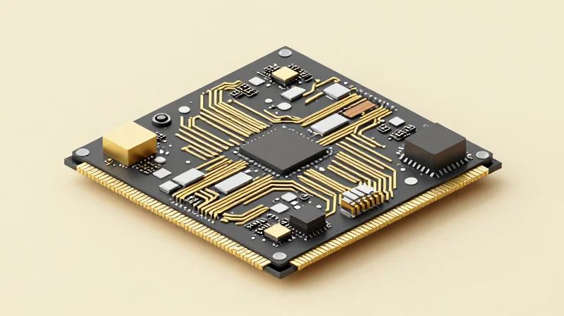
In AED defibrillator designs, the trace path carrying the high-voltage pulse must be engineered to handle high current densities during the milliseconds of discharge. Standard IPC-2221 calculations often prove insufficient for these pulse conditions because the heating is adiabatic; the energy must be dissipated or tolerated without reaching the glass transition temperature (Tg) of the substrate or triggering thermal stress-induced delamination.
Dynamic Thermal Management: Width vs. Copper Weight
| Design Metric | Standard Signal | High-Energy Pulse |
|---|---|---|
| Copper Thickness | 1 oz (35um) | 2 oz to 4 oz (70-140um) |
| Trace Width | Calculated for steady state | Maximized for skin effect/thermal mass |
| Corner Geometry | 90-degree okay | Radiused (Rounded) only |
For pulsed applications, increasing copper weight is generally superior to simply widening the trace. Thicker copper provides higher thermal inertia, absorbing the pulse energy before the substrate interface reaches critical temperatures. However, designers must account for the etch factor, as thicker copper requires wider spacing to maintain adequate insulation gaps and manufacturing yields.
Best Practices for Pulsed Trace Layout
- Why should high-voltage traces use radiused corners?
Right-angle corners create current crowding effects that increase local impedance and create localized thermal hotspots, which can cause substrate lifting or delamination under high-energy discharge. - How does copper thickness affect pulse reliability?
Increased copper thickness provides higher volumetric heat capacity, allowing the trace to absorb the energy pulse without exceeding the bond-strength threshold between the copper foil and the resin substrate. - What is the role of the soldermask in high-energy paths?
For high-voltage paths, it is often recommended to remove soldermask or apply high-voltage-rated conformal coating, as standard masks can carbonize under intense arcing or corona discharge, creating a permanent conductive path.
Ultimately, the design must prioritize current path symmetry. An asymmetric current path induces varying magnetic fields and unequal current distribution across the trace width, leading to localized heating. By implementing radiused bends and ensuring uniform copper distribution, engineers can significantly increase the Mean Time Between Failures (MTBF) for AED discharge modules.
Thermal Management for Power Sections
Thermal Path Optimization for Power MOSFETs
In AED design, power MOSFETs manage the critical high-energy discharge pulses. To prevent thermal runaway, designers must minimize the junction-to-ambient thermal resistance through optimized copper pouring and direct thermal coupling. The primary objective is to move heat away from the silicon die and into the substrate or an external heat sink before it degrades the board's dielectric properties.
Thermal Vias and Copper Pours
Implementing a dense array of thermal vias directly beneath the MOSFET pads allows heat to transfer to inner ground or power planes, which act as heat spreaders. For high-voltage systems, designers should utilize 'plugged and capped' vias to ensure solder integrity and prevent solder wicking, which could create sharp points prone to corona discharge.
| Technique | Primary Benefit | Design Consideration |
|---|---|---|
| Thermal Vias | Lowers Junction Temp | Must be capped for high voltage |
| Copper Pours | Heat Spreading | Avoid excessive area near HV nodes |
| Heat Sinks | Dissipation | Ensure isolation from HV traces |
Component Placement for Thermal Longevity
Strategic component placement isolates high-heat power sections from sensitive control logic and battery management systems. Placing the high-voltage discharge capacitors and MOSFET switches near the edge of the board allows for improved airflow, while ensuring sufficient creepage distances between heated pads and logic-level signals remains a priority.
- How do thermal vias impact dielectric strength?
Thermal vias can introduce stress concentrations; they must be spaced away from high-voltage traces to prevent localized electrical stress that could lead to dielectric breakdown. - Why is heat sinking critical for battery-operated AEDs?
Heat causes internal impedance shifts and chemical degradation in batteries; maintaining a cool operating environment extends the standby and functional life of the device. - Should I use aluminum or copper heat sinks?
Copper offers superior thermal conductivity but is heavier; choose based on the thermal load of your specific discharge circuit and the mechanical constraints of the AED chassis.
EMI/EMC Mitigation in High-Energy Switching Circuits

EMI/EMC Mitigation in High-Energy Switching Circuits
The rapid discharge of high-voltage capacitors in an AED creates extreme dV/dt transients, which can couple into sensitive ECG front-end circuitry via capacitive and inductive pathways. Mitigating this interference requires a multi-layered approach involving strict loop minimization, differential signaling, and strategic isolation to preserve the signal-to-noise ratio of critical diagnostic sensors.
Effective Noise Control Strategies
- Loop Area Reduction
Minimize the physical area of high-current discharge loops by placing the capacitor, switch, and inductor in close, compact proximity to reduce magnetic field radiation. - Galvanic and Impedance Isolation
Utilize opto-isolators or digital isolators to separate the high-voltage discharge controller from the microcontroller, effectively breaking ground loops. - Strategic Guard Tracing
Employ guard traces connected to a low-impedance quiet ground around sensitive high-impedance signal paths to bleed off capacitive coupling from high-voltage transients.
Mitigation Technique Comparison
| Method | Primary Function | Implementation Complexity |
|---|---|---|
| Faraday Shielding | Radiated emission suppression | High |
| Snubber Circuits | Dampens ringing/overshoot | Medium |
| Star Grounding | Prevents common-mode noise | Low |
Designers should also prioritize the use of multi-layer PCB stacks with dedicated solid ground planes beneath the switching section. By ensuring a low-impedance return path directly underneath the high-current traces, the magnetic flux cancellation is maximized, significantly reducing the radiated EMI profile that could otherwise interfere with the device's patient interface.
Strategic Component Placement and Routing
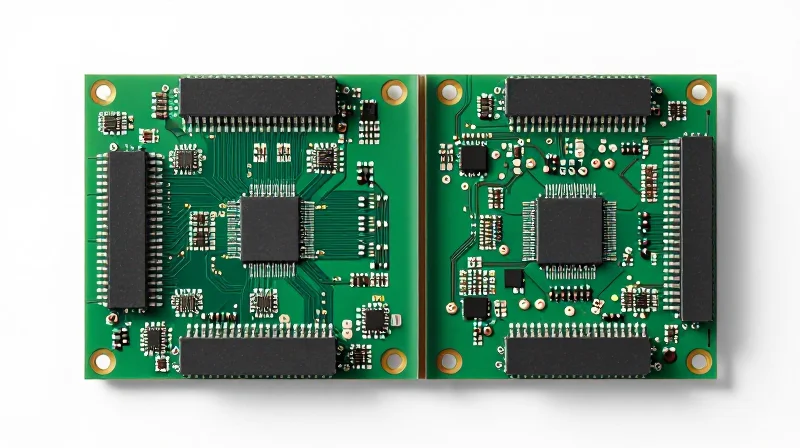
Geometric Isolation and Creepage Management
Effective high-voltage design for AEDs centers on the physical segregation of functional zones. The high-energy discharge section must be isolated from the low-voltage microprocessor and ECG signal acquisition front-end through dedicated keep-out regions and physical board slots to mitigate the risk of dielectric breakdown and arc-over.
Placement Strategies for High-Voltage Reliability
- Energy Storage Concentration
Place high-voltage electrolytic capacitors and discharge transformers at the board periphery to minimize high-energy current loops that could interfere with signal integrity. - Signal Path Protection
Route low-voltage differential pairs away from the discharge path, ensuring that sensitive sensing traces are shielded by ground planes and kept on inner layers where possible. - Component Orientation
Align high-voltage components to optimize thermal dissipation and airflow, ensuring that heat-generating power stages do not affect the drift characteristics of sensitive analog components.
Comparative Routing Standards
| Circuit Zone | Clearance Requirement | Routing Priority |
|---|---|---|
| High-Voltage (DC/Pulse) | IPC-2221 Class B | Shortest Path/Width |
| Control Logic | Standard Signal | Impedance Matched |
| Isolation Barrier | Creepage/Clearance Slot | Dielectric Integrity |
Common Design Challenges
- How does PCB thickness impact high-voltage layout?
Increased thickness improves structural rigidity for heavy power components and provides better dielectric strength, allowing for tighter spacing without risking interlayer breakdown. - Why is slotting essential between power and signal zones?
Routing slots increase the creepage distance along the surface of the PCB, providing a superior barrier against conductive paths created by contamination or moisture.
Validation and Testing Protocols
Verification Through Simulation and Empirical Testing
Validating a high-voltage AED design requires a dual-track approach: virtual simulation to identify thermal and electrical stress points, followed by empirical destructive testing to establish actual failure thresholds. Simulation models, including Finite Element Analysis (FEA) for thermal gradients and SPICE-based modeling for discharge transients, must be performed early to optimize trace widths and creepage distances. However, because AEDs operate in critical life-support scenarios, analytical models must be calibrated against physical prototypes subjected to extreme environmental and electrical conditions to ensure long-term robustness.
Destructive and Accelerated Life Testing Protocols
To ensure compliance with medical safety standards (such as IEC 60601-2-4), designers must move beyond functional testing and employ accelerated stress testing to verify the board's structural integrity.
| Test Type | Objective | Key Indicator |
|---|---|---|
| Highly Accelerated Life Testing (HALT) | Identify weak points via thermal/vibration stress | Time-to-failure (TTF) |
| High-Voltage Dielectric Withstand | Verify insulation and clearance integrity | Leakage current stability |
| Thermal Shock Cycling | Check solder joint fatigue from rapid discharge | Interconnect resistivity |
Frequently Asked Questions on AED Board Validation
- How does destructive testing account for high-voltage arc-over?
Destructive testing uses specialized atmospheric chambers that simulate high humidity and varied air pressures to force insulation breakdown, allowing engineers to verify the effectiveness of conformal coatings and physical isolation barriers. - At what stage should simulation data be locked?
Simulation should be treated as a live document, finalized only after it correlates within 5-10% of the physical measurements obtained from the Alpha prototype testing phase. - Is standard functional testing sufficient for AEDs?
No, standard functional testing only ensures the device works under nominal conditions; robust AED design requires stress-testing for transient energy spikes that occur during internal defibrillation discharge cycles.
Designing for high-voltage medical hardware is a complex journey, but by adhering to these stringent DFM rules and safety standards, you ensure your device remains both reliable and life-saving. Don't leave your compliance to chance—partner with our expert engineering team today to audit your PCB design and accelerate your path to market. Contact us now to start your prototype review.
