
As the demand for ultra-compact, multifunctional wearables surges, the heartbeat of your device—the PCB—faces unprecedented pressure. R&D teams are no longer just fighting for board space; they are battling to balance electrical performance, mechanical flexibility, and long-term reliability. Choosing between Rigid-Flex and High-Density Interconnect (HDI) architectures is the definitive fork in the road for modern hardware engineers.
The Current Landscape of Wearable PCB Engineering
The evolution of wearable technology has transitioned from simple step-counting pedometers to complex, multi-modal health monitoring platforms. This shift has placed immense pressure on printed circuit board (PCB) design, where engineers must balance aesthetic minimalism with high-performance electrical requirements. The current landscape is defined by a race toward maximum volumetric efficiency, where every cubic millimeter of housing must be optimized to accommodate dense sensor suites, high-capacity batteries, and robust wireless connectivity.
Key Drivers of High-Density Requirements
Modern fitness trackers now incorporate sophisticated features that were previously reserved for higher-end mobile devices. These advancements necessitate architectures that can handle high-speed data transmission and sensitive analog signal processing within a drastically reduced form factor.
- Multi-Sensor Fusion
Continuous heart rate (PPG), blood oxygen (SpO2), and skin temperature sensors require high-precision analog front-ends that occupy significant board real estate. - Integrated GNSS
Embedding GPS/GLONASS modules requires careful RF routing and shielding to prevent noise interference with low-power biometric sensors. - Power Management
Smaller, high-energy-density batteries force power regulation components into tight clusters, increasing thermal management complexity.
Comparing Architectural Approaches
| Feature | Rigid-Flex PCB | HDI (High-Density Interconnect) |
|---|---|---|
| Form Factor Flexibility | High (3D shaping) | Low (Fixed planar) |
| Routing Complexity | Moderate | Very High |
| Unit Cost | High | Moderate |
| Mechanical Reliability | Superior | Standard |
As the industry matures, the choice between rigid-flex and HDI solutions becomes a strategic trade-off. Rigid-flex designs are increasingly favored for devices that require irregular, wearable-specific ergonomics, effectively replacing cables and connectors with a singular, durable interconnect structure. Conversely, HDI technology remains the workhorse for flat, high-density logic boards, providing the trace density necessary to support modern microcontrollers and high-speed memory interfaces.
Understanding High-Density Interconnect (HDI) Design
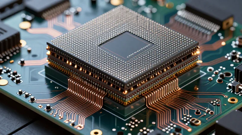
Defining High-Density Interconnect (HDI)
HDI technology represents a leap forward from standard PCB manufacturing by utilizing advanced laser drilling and imaging processes to achieve higher wiring density per unit area. By shrinking trace widths, spacing, and via diameters, HDI boards allow designers to place complex components like System-on-Chips (SoCs) and biometric sensors in ultra-compact footprints without sacrificing electrical performance or reliability.
Core HDI Enablers
| Technology Feature | Functional Impact |
|---|---|
| Microvias | Small-diameter laser-drilled holes that allow for signal transitions between adjacent layers. |
| Blind/Buried Vias | Vertical interconnects that connect inner layers without penetrating the entire board stack, conserving surface real estate. |
| Fine-Line Technology | Advanced copper etching processes producing trace widths/spacings below 75 microns. |
HDI Design Considerations for Wearables
- How do microvias improve signal integrity?
Microvias reduce the 'stub' length effect found in traditional through-hole vias, which minimizes parasitic capacitance and inductance—critical factors for high-speed sensor data. - What is the primary constraint when moving to HDI?
The primary constraint is manufacturing cost; HDI requires precise registration and specialized laser equipment compared to standard multi-layer manufacturing processes. - Why is layer stack-up efficiency vital?
In fitness trackers, vertical space is limited. HDI allows for 'any-layer' via configurations, enabling a much thinner board profile while maintaining high component density.
Adopting HDI is not merely a design choice but a requirement for modern wearable engineering. As fitness devices integrate more complex power management and global connectivity, the ability to pack more functionality into thinner, lighter packages through HDI becomes the competitive edge for hardware developers.
The Rise of Rigid-Flex Circuits in Mobile Electronics
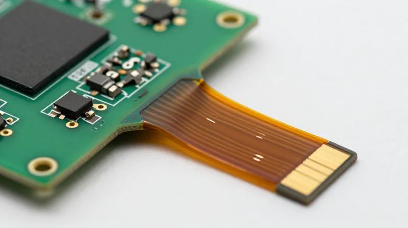
The Rise of Rigid-Flex Circuits in Mobile Electronics
As fitness trackers evolve toward smaller form factors and more ergonomic designs, the traditional rigid PCB approach has become a bottleneck. Rigid-flex circuits solve this by utilizing flexible polyimide layers that allow the board to fold, twist, and contour within the chassis of a wearable device. By replacing rigid-to-flex ribbon cables with an integrated, single-unit construction, manufacturers can drastically reduce failure points while reclaiming critical space for battery capacity and advanced sensor arrays.
Strategic Advantages for Modern Wearables
| Feature | Rigid-Flex Advantage | Impact on Fitness Trackers |
|---|---|---|
| Mechanical Reliability | Eliminates connectors | Resists shock and vibration |
| Volumetric Efficiency | Dynamic 3D folding | Increased battery life |
| Interconnect Integrity | Single-board assembly | Reduced signal impedance |
The integration of polyimide materials allows the circuit to act as both a PCB and a cable simultaneously. This eliminates the need for bulky ZIF or board-to-board connectors that often represent the weakest point in a wearable's structural integrity. By treating the interconnect as a structural element, engineers can pack more functionality into thinner, more comfortable bands that conform naturally to the human wrist.
- Why is polyimide used in rigid-flex?
Polyimide provides superior thermal stability and mechanical flexibility, ensuring the substrate can undergo repetitive folding without fracturing or degrading electrical performance. - How does rigid-flex compare to HDI in cost?
While rigid-flex fabrication is generally more expensive than pure HDI, it provides significant cost offsets through assembly automation and decreased mechanical housing complexity. - Does rigid-flex support high-speed signals?
Yes, because rigid-flex eliminates the parasitic inductance and capacitance introduced by physical connectors, it often provides cleaner signal paths for high-frequency biometric data.
Direct Comparison: Component Density and Real Estate
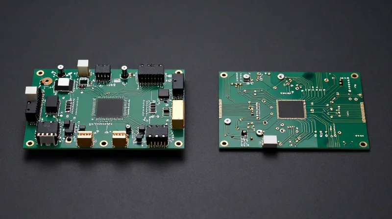
Direct Comparison: Component Density and Real Estate
The choice between HDI and rigid-flex is a trade-off between absolute surface area reduction and three-dimensional spatial utilization. While HDI focuses on compressing circuits into a smaller flat footprint via aggressive layer stacking and microvia technology, rigid-flex focuses on leveraging the device enclosure by folding the PCB to fit unconventional geometric volumes, effectively eliminating the need for bulky rigid-to-rigid interconnects.
| Feature | HDI PCB | Rigid-Flex PCB |
|---|---|---|
| Primary Advantage | Extreme surface density | Volumetric space efficiency |
| Space Strategy | 2D miniaturization | 3D structural integration |
| Connection Reliability | Standard SMT assembly | Higher due to eliminated connectors |
| Best Application | Dense, flat wearables | Curved, ergonomic fitness bands |
Optimizing Real Estate in Fitness Trackers
In modern fitness trackers, designers are moving away from traditional rectangular layouts. Rigid-flex boards excel here by allowing the electronics to wrap around the wrist or conform to rounded sensor housings. Conversely, HDI technology remains the gold standard for high-performance processing modules where raw computational density and signal integrity for advanced biometric processing take precedence over board shape conformability.
- Which technology allows for a smaller total device volume?
Rigid-flex often wins in total volume reduction because it allows the PCB to replace physical housing segments and eliminate bulky cable connectors, effectively using the device's internal chassis as part of the board structure. - Does HDI negate the need for rigid-flex in compact trackers?
No; while HDI allows for more components on a single square inch, it cannot solve the problem of interconnecting multiple boards placed at different angles within a non-linear enclosure as effectively as rigid-flex can.
Signal Integrity and Thermal Management Considerations
Optimizing Signal Integrity in Wearables
Maintaining signal integrity is the primary hurdle as fitness trackers integrate high-speed sensors and Bluetooth Low Energy (BLE) antennas. HDI designs excel in signal containment due to their sophisticated stack-up capabilities, which allow for shorter trace lengths and optimized ground plane referencing. By utilizing microvias, HDI technology minimizes parasitic inductance, essential for preserving the integrity of high-frequency data signals. In contrast, rigid-flex boards introduce discontinuities at the transition between rigid and flexible substrates, which can create impedance mismatches. Careful control of trace geometry and dielectric spacing across these flex joints is vital to preventing signal reflection in modern wearable architectures.
Thermal Management and Heat Dissipation
As component density increases, thermal management transitions from a passive concern to an active design constraint. HDI boards, typically featuring more internal copper layers, provide superior heat spreading across the device's mainboard. However, rigid-flex circuits offer a unique advantage by allowing heat-generating components to be mounted on separate rigid islands, effectively decoupling them from sensitive thermal-sensitive sensors. The flexible sections, while thin, do not facilitate heat transfer as efficiently, meaning that thermal relief must be strategically engineered using thermal vias and copper pouring patterns.
| Feature | HDI PCB Performance | Rigid-Flex Performance |
|---|---|---|
| Signal Integrity | Excellent (Short paths, low parasitics) | Requires careful transition impedance matching |
| Heat Dissipation | Superior (High internal copper density) | Localized (Component isolation possible) |
| EMI Shielding | High (Better ground plane layering) | Moderate (Requires flex-specific shielding) |
Design Considerations FAQ
- How do microvias impact signal noise?
Microvias reduce the electrical path length compared to through-hole vias, significantly lowering the inductance and capacitive coupling that cause signal crosstalk. - Is rigid-flex material thermally stable?
Standard polyimide flex materials have lower thermal conductivity than FR-4 rigid boards, making careful thermal modeling of the rigid sections critical. - Does higher density increase thermal risk?
Yes, increasing component density without increasing substrate copper thickness leads to localized heat pockets, requiring thermal via arrays to bridge heat to ground planes.
Reliability and Mechanical Fatigue in Daily Wear

Mechanical Fatigue and Dynamic Stress Management
Fitness trackers are subjected to constant mechanical strain, including vibration, torsion, and cyclic bending. Rigid-flex PCBs excel in this environment by integrating flexible polyimide circuits that decouple rigid sections, effectively absorbing mechanical stress. In contrast, high-density interconnect (HDI) boards, while mechanically robust, are rigid in nature; they are highly susceptible to solder joint fracturing when integrated into form factors that undergo repetitive thermal expansion or physical deformation.
| Failure Mode | Rigid-Flex Resilience | HDI Board Resilience |
|---|---|---|
| Vibration Resistance | High: Flex zones dampen energy | Low: Rigidity stresses joints |
| Repetitive Bending | Excellent: Tested for millions of cycles | Critical: Prone to crack propagation |
| Thermal Expansion | High: Polyimide accommodates CTE | Moderate: Vulnerable at connector interfaces |
Design Considerations for Reliability
To maximize lifespan, engineers must employ specific layout techniques to mitigate fatigue. For rigid-flex, the transition zones (bends) must be designed with curved traces and offset pads to prevent copper work-hardening. For standard HDI, reliability is often compromised by the use of connectors; replacing board-to-board connectors with direct-soldered rigid-flex interfaces significantly reduces the potential for contact oxidation and connection failure in sweat-heavy or high-moisture environments.
- How does polyimide affect fatigue life?
Polyimide acts as a flexible substrate that inherently resists micro-cracking and maintains structural integrity far longer than traditional FR-4 materials under repeated cyclic strain. - Why do HDI boards struggle with mechanical shock?
Because HDI boards are fundamentally rigid, they transfer all kinetic energy directly to the surface-mounted solder joints, leading to intermetallic bond failure over time. - Is rigid-flex always the more reliable choice?
While superior for dynamic movement, rigid-flex requires more stringent manufacturing tolerances. If the bend radius is too tight, the material may exceed its elastic limit, resulting in permanent damage.
Cost-to-Performance Analysis for Mass Manufacturing
Economic Implications of PCB Selection
Transitioning from traditional HDI to rigid-flex architecture requires a careful analysis of the Bill of Materials (BOM) and total manufacturing yield. While rigid-flex offers superior mechanical flexibility and space utilization, it introduces significant complexity into the fabrication process, often resulting in higher per-unit costs compared to standard multilayer HDI boards.
| Metric | Standard HDI | Rigid-Flex |
|---|---|---|
| Material Cost | Low to Moderate | High |
| Fabrication Complexity | Moderate | High |
| Assembly Efficiency | High | Moderate |
| Unit Yield | Very High | Moderate |
Key Cost Drivers in Mass Production
In mass production, the cost gap between these technologies is primarily driven by process steps and assembly overhead. HDI designs benefit from established, high-volume manufacturing lines that feature excellent economies of scale. Conversely, rigid-flex fabrication requires specialized lamination processes, complex drilling sequences, and meticulous handling during assembly to prevent damage to delicate flexible sections.
- Why is rigid-flex more expensive to manufacture?
The requirement for specialized adhesive materials, polyimide coverlays, and multi-stage lamination cycles significantly increases direct material and processing costs. - Does HDI offer better cost efficiency for high-volume trackers?
Yes, standard HDI boards leverage mature manufacturing infrastructure, resulting in lower fabrication costs and higher throughput rates for high-volume consumer devices. - How does PCB choice impact assembly automation?
Rigid-flex boards often necessitate custom assembly jigs and fixtures to maintain board geometry during pick-and-place, adding to the non-recurring engineering (NRE) and operational expenses.
For designers, the decision must balance the product's premium positioning against manufacturing overhead. If the fitness tracker requires extreme form-factor miniaturization where standard HDI cannot satisfy the enclosure constraints, the performance gains of rigid-flex justify the investment. However, for cost-sensitive market segments, optimizing an HDI design remains the most effective strategy to preserve profit margins.
Future-Proofing Your Product Roadmap
Architectural Scalability for Future Wearables
Future-proofing a fitness tracker roadmap involves designing for the 'sensor-to-battery' gap. As devices shift from basic activity tracking to medical-grade health monitoring—incorporating ECG, SpO2, and continuous glucose monitoring—the PCB footprint must accommodate denser circuitry without sacrificing the mechanical flexibility required for ergonomic wear. Architects must choose a substrate platform that avoids 'design debt' by ensuring signal integrity remains stable as data throughput requirements double.
Strategic Selection Criteria
| Feature | Rigid-Flex Advantage | HDI Stacked-Via Advantage |
|---|---|---|
| Sensor Integration | Superior 3D spatial mapping | High-density interconnect density |
| Battery Capacity | Allows curved battery shapes | Maximizes board-level component space |
| Technology Lifecycle | Best for non-rectangular form factors | Best for iterative performance upgrades |
Frequently Asked Questions
- Which technology better supports miniaturized batteries?
Rigid-flex PCBs offer a superior advantage here, as the flexible interconnects allow for non-planar battery placement, effectively utilizing the entire internal casing volume of the wearable. - Is HDI more sustainable for long-term product iterations?
HDI designs are generally more sustainable for incremental iterations because the standardized manufacturing processes allow for easier component swaps and board-level updates compared to the complex lamination cycles of rigid-flex. - How does signal integrity affect roadmap longevity?
As fitness trackers adopt high-speed wireless protocols, HDI boards provide better controlled-impedance environments, which is critical for reducing signal noise as sensor data resolution increases over product generations.
Selecting the right PCB architecture is a strategic decision that influences everything from your time-to-market to your device's failure rate. While HDI remains the gold standard for high-density stationary electronics, the unique mechanical requirements of wearables often tilt the balance toward rigid-flex. Ready to refine your hardware strategy? Contact our engineering team today to review your current PCB stack-up and optimize your roadmap for the next generation of wearable tech.
