
In the fast-paced world of wearable and portable medical technology, the traditional PCB footprint is shrinking while the demand for high-fidelity data intelligence is skyrocketing. As engineers transition away from legacy thermistor-based thermal sensing, understanding the architectural implications of modern digital sensors is no longer optional—it is a competitive necessity.
The Anatomy of Modern PCBA Miniaturization
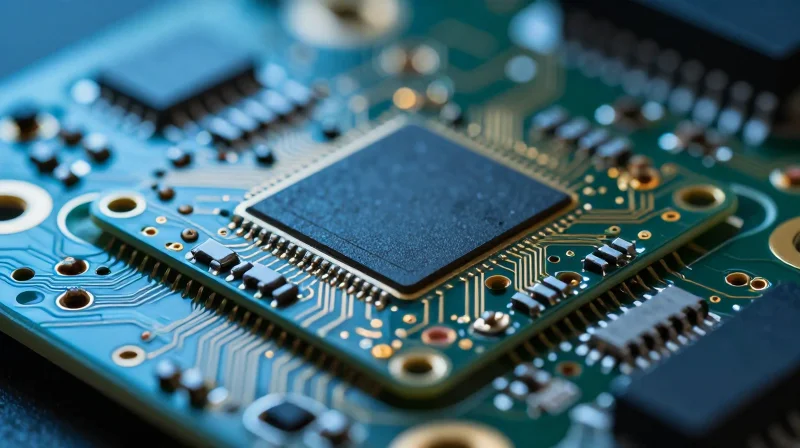
Drivers of PCBA Miniaturization
The evolution of thermal sensing is inextricably linked to the demand for compact, wearable, and IoT-enabled devices. As the required form factors for modern digital thermometers and environmental sensors shrink, the underlying Printed Circuit Board Assembly (PCBA) must accommodate increasing complexity within a diminished physical footprint. This trend is driven by the necessity for reduced latency, lower power consumption, and the integration of multi-modal sensing capabilities into single, highly miniaturized packages.
High-Density Interconnects (HDI) and Material Evolution
To achieve these tighter specifications, designers are moving away from legacy rigid board architectures toward High-Density Interconnect (HDI) technology. HDI enables higher circuit density through the use of micro-vias, thinner lines, and smaller capture pads, effectively allowing more functionality per square millimeter. Furthermore, the migration toward advanced substrate materials with lower dielectric constants is essential to maintain signal integrity while reducing the total board stack-up, a critical factor when dealing with the high-precision analog signals common in thermal measurement.
| Feature | Legacy PCBA | Modern Miniaturized PCBA |
|---|---|---|
| Via Technology | Thru-hole | Laser-drilled Micro-vias |
| Trace/Space | 5-6 mils | < 3 mils |
| Integration | Discrete components | System-in-Package (SiP) |
| Thermal Path | Bulk conduction | Optimized micro-thermal vias |
Frequently Asked Questions on PCBA Miniaturization
- How does miniaturization impact thermal sensitivity?
Smaller footprints reduce thermal mass, allowing sensors to respond more rapidly to ambient temperature shifts, but they also require more sophisticated PCB design to isolate the sensor from heat-generating components. - Why are system-in-package (SiP) solutions favored?
SiP solutions combine the microcontroller, sensor interface, and passive components into a single package, drastically reducing board real estate and minimizing parasitic effects. - What is the biggest design challenge in compact PCBAs?
The primary challenge is balancing signal integrity and heat dissipation in a confined space where trace routing is restricted and thermal crosstalk between components is significantly higher.
Legacy Limitations: Why Thermistors Are Being Phased Out
Inherent Calibration and Nonlinearity Constraints
Thermistors, while cost-effective for legacy applications, present significant engineering hurdles due to their highly nonlinear resistance-temperature characteristics. The reliance on the Steinhart-Hart equation or complex look-up tables to convert raw resistance into meaningful temperature data creates a substantial computational overhead for microcontrollers. Unlike modern digital sensors that output processed data over standardized protocols like I2C or SPI, thermistors require precision analog front-end (AFE) components, including high-accuracy reference resistors and noise-filtering stages, which consume valuable PCBA real estate.
Comparative Limitations of Sensing Technologies
| Feature | Legacy Thermistor | Modern Digital Sensor |
|---|---|---|
| Signal Conditioning | External AFE Required | Integrated ADC/Digital Logic |
| Output Format | Analog (Resistance) | Digital (I2C/SPI/SMBus) |
| Calibration Needs | High (Nonlinear Curves) | Minimal (Factory Trimmed) |
| PCBA Footprint | Large (Includes discrete passives) | Small (Monolithic IC) |
Engineering FAQ: Moving Beyond Thermistors
- Why do thermistors require more space on a PCB?
Thermistors act as passive components, requiring supporting circuitry such as voltage dividers, noise-reduction capacitors, and precision reference resistors to convert resistance into an analog signal for the ADC. - What is the primary risk of using thermistors in mass production?
Manufacturing variance and the need for individual board-level calibration can significantly increase total cost of ownership and assembly time compared to pre-calibrated digital sensors. - Does digital sensing affect power consumption?
Digital sensors often include integrated power management features like ultra-low-power sleep modes and programmable sample rates, which are inherently more efficient than keeping an analog AFE chain constantly biased.
The Rise of Digital Sensor Integration

The Shift to Digital Bus Architecture
The evolution of thermal sensing is fundamentally defined by the transition from analog voltage-divider circuits to high-speed digital bus communication. By integrating the sensing element, the reference, and the analog-to-digital converter (ADC) onto a single silicon die, modern digital sensors communicate directly with the microcontroller (MCU) via standardized protocols like I2C or SPI. This architectural shift eliminates the need for external ADC stages, complex shielding, and precision resistor networks that historically occupied significant PCB real estate.
Comparative Efficiency of Thermal Sensing Architectures
| Feature | Legacy Thermistor PCBA | Digital Sensor PCBA |
|---|---|---|
| External ADC Required | Yes | No (Integrated) |
| PCB Routing Complexity | High (Analog traces) | Low (Digital Bus) |
| Signal Calibration | Manual/Resistance-based | Factory-Calibrated Digital |
| Noise Sensitivity | High (Analog) | Low (Digital Logic) |
Technical Advantages for PCB Routing
Digital sensors significantly simplify board layout by treating thermal data as packets rather than raw analog signals. Because I2C and SPI are inherently more noise-immune than sensitive analog voltage signals, engineers are no longer required to implement intricate guard-tracing or isolate thermal traces from high-frequency interference. This allows for tighter component placement and increased density in space-constrained IoT or medical-grade devices.
- Does digital sensor integration improve system reliability?
Yes, by removing discrete signal conditioning circuitry, you reduce the overall bill of materials (BOM) and the number of failure points, while factory-calibrated digital sensors eliminate the need for costly manual tuning on the production line. - How does I2C affect power consumption?
Digital sensors typically feature ultra-low power standby modes and support high-speed burst reading, allowing the sensor to remain dormant for the majority of the duty cycle, significantly extending battery life in wireless thermal monitoring applications.
Precision vs. Power: Evaluating Performance Metrics
Precision vs. Power: Evaluating Performance Metrics
Optimizing thermal sensing performance in portable medical devices necessitates a nuanced understanding of the trade-offs between computational overhead and power budgets. While high-resolution digital sensors offer superior precision, they often demand higher peak current during active sampling cycles, necessitating a design strategy that prioritizes optimized duty cycling and ultra-low-power sleep states.
Quantitative Comparative Analysis
| Metric | Digital ASIC Sensor | Legacy Thermistor Circuit | Emerging MEMS Thermal |
|---|---|---|---|
| Typical Accuracy | ±0.1°C to ±0.5°C | ±0.5°C to ±1.0°C | ±0.05°C |
| Power Consumption | 2µA - 10µA (Avg) | 100µA+ (Voltage Divider) | <1µA (Deep Sleep) |
| Drift Stability | Negligible (Factory Cal) | High (Requires Aging) | Low |
| Signal Conditioning | Digital Bus (I2C/SPI) | External ADC Required | Integrated Logic |
Critical Implementation Considerations
- How does sensor resolution impact battery life?
Higher resolution sensors require longer integration times or increased sampling rates to process signal noise, which directly increases the mA-per-second draw during measurement cycles. - Why is long-term drift a primary concern for PCBAs?
In medical devices, drift necessitates periodic recalibration; digital sensors mitigate this with EEPROM-stored coefficients, whereas traditional thermistors degrade based on thermal cycling exposure. - What role does the bus interface play in power management?
I2C/SPI interfaces allow for 'event-driven' wake-up; the sensor remains in standby until requested, minimizing the time the MCU spends in active power modes compared to constant analog monitoring.
Smart-Connected Capabilities and Edge Processing

Local Data Analytics at the Edge
Modern digital sensor nodes have shifted from passive data acquisition to active, localized intelligence. By moving processing logic onto the PCBA via micro-controllers or intelligent digital sensor ICs, thermal devices can filter noise, perform trend analysis, and calculate rates of temperature change locally. This capability drastically reduces the data throughput required for downstream transmission, optimizing battery life and bandwidth in wireless applications.
Connectivity and Real-Time Performance
Integrating thermal sensors with wireless protocols such as BLE (Bluetooth Low Energy) or Wi-Fi necessitates a careful balance between connectivity cycles and sensor sampling latency. Newer architectures utilize low-power interrupts and hardware-based event monitoring to ensure that the system maintains real-time response capabilities even when the main processor is in a deep sleep state, preserving the fidelity of critical measurements.
| Feature | Legacy PCBA Design | Smart-Connected PCBA |
|---|---|---|
| Processing | Centralized (Host CPU) | Edge (On-Sensor or Local MCU) |
| Communication | Wired Analog/Digital | Wireless IoT/MQTT |
| Data Handling | Raw Data Streaming | Event-Based Analytics |
| Power Efficiency | Low (High Latency) | High (Hardware Intercepts) |
Frequently Asked Questions on Edge Sensing
- Does edge processing impact measurement accuracy?
No; in fact, it often improves it by allowing for real-time digital compensation and drift calibration within the sensor node itself before data transmission. - How is real-time performance maintained during wireless transmission?
High-performance architectures utilize asynchronous sampling buffers, ensuring that the critical thermal capture loop remains uninterrupted by the non-deterministic timing of wireless packet stacks. - Is cloud connectivity necessary for local analysis?
Edge processing allows for autonomous operation, meaning the device can trigger alarms or adjustments locally without waiting for cloud handshakes.
Thermal Management in High-Density Assemblies
Managing Thermal Crosstalk in Compact PCB Layouts
As designers push for smaller form factors, the primary challenge shifts from general cooling to preventing thermal crosstalk, where heat from high-power components skews the precision of adjacent digital thermometers. In high-density assemblies, thermal isolation becomes as critical as electrical signal integrity. Relying on digital sensors with internal calibration features is no longer sufficient if the physical substrate acts as a conduit for unintended heat transfer.
Mitigation Strategies for Localized Heat
- Thermal Vias and Ground Planes
Utilizing arrays of micro-vias under sensor pads connects them to internal copper planes, effectively spreading localized heat and creating a lower-impedance thermal path away from sensitive sensing elements. - Component Partitioning
Strategic layout planning should place high-power switching regulators on the opposite side of the PCB or at maximum physical distance from high-precision thermal nodes to prevent convective drift. - Thermally Conductive Underfill
In extremely dense designs, using specialized underfills can stabilize the interface between the sensor and the PCB, ensuring the sensor tracks the board temperature rather than the ambient air flow.
Comparative Efficiency of Thermal Management Techniques
| Technique | Primary Benefit | Implementation Complexity |
|---|---|---|
| Copper Thermal Vias | Heat Spreading | Low |
| Substrate Slitting | Thermal Isolation | High |
| Active Heat Sinking | High-Flux Dissipation | Moderate |
| Intelligent Calibration | Software Compensation | Low |
When comparing traditional PCBAs to emerging sensor technologies, the shift is moving toward integrated digital solutions that offer built-in compensation algorithms. These modern sensors allow firmware-level adjustments to account for known board hot spots, effectively providing a digital 'buffer' against the physical realities of high-density assembly design.
Strategic Component Sourcing for Medical Compliance
Regulatory Integrity and Component Traceability
In the medical sector, the selection of thermal sensing components is not merely a technical decision but a regulatory one. Under ISO-13485, every component integrated into a PCBA must be traceable to its origin. Strategic sourcing requires that manufacturers demand full material declarations (FMD) and certificates of conformance (CoC) from suppliers. Failure to verify the pedigree of critical sensors can lead to batch rejections, product recalls, and severe legal liabilities, especially when transitioning from off-the-shelf components to custom-engineered sensor arrays.
Supply Chain Resilience and Risk Mitigation
| Sourcing Strategy | Risk Factor | Compliance Impact |
|---|---|---|
| Single-Source Custom Sensors | High dependency/Lead time | Requires extensive qualification |
| Multi-Vendor Standard PCBAs | Inconsistent calibration | High validation overhead |
| Strategic Partnership | Lower agility | Streamlined audit trails |
Frequently Asked Questions on Sourcing Compliance
- How does ISO-13485 affect vendor selection?
ISO-13485 requires a documented process for the evaluation and selection of suppliers based on their ability to meet quality requirements and maintain regulatory documentation standards. - Why is component obsolescence a critical issue for thermal sensors?
Medical devices often have 5-10 year lifecycles; if a sensor is discontinued, re-validating a new component requires expensive design changes and potentially a full regulatory re-certification. - What documentation must be archived for auditing?
You must maintain technical files including sensor data sheets, calibration logs, RoHS/REACH compliance certificates, and evidence of periodic supplier quality audits.
Future-Proofing Your Next Device Design
Designing for Scalability and Lifecycle Management
To future-proof your next medical device, shift from rigid, monolithic PCBAs to modular, interface-driven hardware architectures. By decoupling the sensing element from the core processing unit, designers can upgrade individual components—such as transitioning from traditional thermistors to advanced MEMS thermal sensors—without requiring a complete redesign of the host platform. This approach protects your investment, eases regulatory re-certification, and allows for rapid feature deployment as sensor technology advances.
Comparison of Design Architectures
| Architectural Approach | Future-Proofing Capability | Design Complexity |
|---|---|---|
| Monolithic PCB | Low - high replacement cost | Low |
| Modular/Bus-based | High - swappable modules | Medium |
| System-on-Chip (SoC) Hybrid | Medium - flexible firmware | High |
Anticipating Next-Generation Patient Requirements
As the industry shifts toward remote patient monitoring and preventative care, the demand for non-contact and continuous thermal sensing is growing. Future designs must account for higher sampling rates, edge-based signal processing to filter artifacts in ambulatory environments, and secure, low-latency connectivity. Integrating flexible interconnects and open-standard communication protocols ensures the device remains compatible with future IoT gateways and clinical dashboard software.
- How can I ensure long-term availability of components?
Prioritize vendors with long-term support (LTS) programs and utilize footprint-compatible components that allow for hardware drop-in replacements if specific sensor models are discontinued. - What role does firmware play in future-proofing?
Firmware-centric designs allow for calibration updates, improved filtering algorithms, and security patches over the air (OTA), significantly extending the usable life of the hardware. - How do I balance miniaturization with future expansion?
Reserve additional PCB real estate or utilize mezzanine connectors even if the current design doesn't require extra processing power, allowing for later addition of wireless modules or auxiliary sensors.
The transition to digital sensing is more than a technical upgrade; it is a fundamental shift toward creating more intuitive, reliable, and portable medical solutions. By prioritizing integrated digital architectures, design teams can overcome the spatial and connectivity bottlenecks of the past. Are you ready to optimize your device's thermal sensing stack? Contact our engineering consultants today to discuss your next PCBA architecture project.
