
The demand for photorealistic spatial computing is pushing current hardware to its absolute limit. With users requiring higher refresh rates and near-zero motion-to-photon latency, traditional PCB architectures have become a bottleneck. To deliver seamless immersion, engineers must pivot toward advanced interconnect solutions. This guide examines how rigid-flex boards and substrate-like PCBs (SLP) are redefining the structural and electrical backbone of modern AR/VR devices.
The Changing Landscape of Spatial Computing Hardware

The Convergence of High Density and Low Latency
As AR/VR headsets transition toward 8K-per-eye resolution and refresh rates exceeding 120Hz, the underlying electronics must process massive data streams within incredibly tight latency budgets. Legacy rigid PCB architectures are increasingly incapable of supporting the signal integrity required for such high-speed data transfer. Engineers are now forced to integrate advanced substrate technologies—such as mSAP (modified Semi-Additive Process) and HDI (High-Density Interconnect)—to minimize trace widths and parasitic capacitance.
Thermal Management Challenges in Compact Form Factors
Spatial computing devices present an inherent conflict: the need for high-performance SoCs and displays against the physical limitations of a wearable device that must dissipate heat away from the user's face. Traditional dielectric materials often fail to provide the necessary thermal conductivity under continuous load. The shift toward specialized low-loss laminates and metal-core PCB integration is critical to preventing thermal throttling, which remains the primary enemy of consistent user immersion.
| Parameter | Legacy PCB | Spatial Computing Substrate |
|---|---|---|
| Trace Width/Spacing | 75-100 μm | 20-30 μm (mSAP) |
| Signal Loss | Moderate/High | Ultra-Low (Low Df/Dk) |
| Component Density | Low | High (Multi-tier HDI) |
| Thermal Conductivity | Standard FR4 | Ceramic-Filled/Metal-Core |
Key Engineering Considerations
- Why is mSAP becoming the industry standard?
mSAP allows for finer copper patterns and straighter sidewalls compared to traditional subtractive etching, which is vital for maintaining signal integrity at the multi-gigabit speeds required by high-resolution displays. - How do dielectric materials impact immersion?
Lower dissipation factors (Df) reduce signal attenuation over high-speed differential pairs, ensuring that data packets reach the display controllers without corruption, thereby eliminating visual artifacts that break immersion. - Is rigid-flex design necessary?
Yes. Spatial computing requires folding high-density circuitry into ergonomic, non-planar headset geometries while minimizing bulky cable connectors, which introduces mechanical and electrical complexity.
Limitations of Standard High-Density Interconnects (HDI)
The Bottlenecks of Legacy HDI Architectures
Standard HDI technology, while revolutionary for smartphone miniaturization, encounters a 'scaling wall' when applied to the next generation of AR/VR headsets. As pixel densities climb toward 8K-per-eye and refresh rates push past 120Hz, standard HDI designs suffer from excessive signal crosstalk, impedance discontinuities, and thermal bottlenecks that hinder immersive performance.
| Parameter | Standard HDI Limitation | Impact on AR/VR Hardware |
|---|---|---|
| Trace Density | Limited layer count/spacing | Increased footprint and weight |
| Signal Integrity | Higher dielectric loss at GHz | Latency and visual artifacting |
| Thermal Flow | Poor heat dissipation via vias | Performance throttling under load |
Addressing Signal Integrity and Thermal Constraints
The fundamental reliance on sequential lamination processes in standard HDI limits the ability to incorporate ultra-fine pitch components without significant signal degradation. In an AR/VR environment, where every millisecond of latency disrupts the vestibular-ocular reflex, the insertion loss inherent in standard laminates becomes unacceptable.
- Why does signal integrity degrade in standard HDI?
Increased trace density leads to electromagnetic interference and crosstalk that standard HDI material sets cannot adequately suppress at the high frequencies required for UHD video transmission. - How does PCB thickness affect headset ergonomics?
Standard HDI requires more layers to route high-speed signals, increasing board thickness and weight, which shifts the center of gravity and reduces user comfort during extended wear. - Can standard HDI handle high-power SoC heat dissipation?
The thermal conductivity of standard dielectric materials is often too low, leading to localized heat spots that throttle processing power and require bulky, heavy cooling solutions.
Rigid-Flex Circuits: The Structural Backbone of Headsets
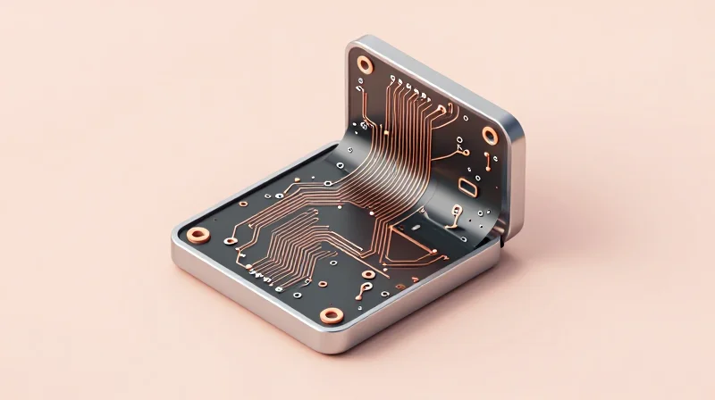
The Synergy of Mechanical Versatility and Electronic Performance
Rigid-flex technology serves as the structural backbone for AR/VR hardware by merging the reliability of rigid PCBs with the space-saving benefits of flexible polyimide circuits. In head-mounted displays (HMDs), where space is at a premium and weight distribution is critical, rigid-flex allows engineers to wrap circuitry around optical components and adjust to ergonomic curves without the need for bulky connectors or fragile cable assemblies.
Optimizing Signal Integrity and Thermal Management
The primary advantage of replacing discrete connectors with integrated rigid-flex traces is the significant improvement in signal integrity. High-speed data lanes—required for 8K-per-eye resolutions and low-latency tracking—suffer from impedance discontinuities at traditional connector pins. By utilizing a continuous, seamless connection from the main board to sensors and displays, engineers mitigate signal degradation and electromagnetic interference (EMI). Furthermore, the thin, flexible portions of these circuits provide better surface area-to-volume ratios, aiding in heat dissipation within the constrained enclosure.
| Feature | Legacy Interconnects | Rigid-Flex Circuits |
|---|---|---|
| Space Efficiency | Low (Connector bulk) | High (Thin-profile flex) |
| Reliability | Moderate (Connector failure) | High (Soldered integration) |
| Signal Path | Interrupted | Continuous |
| Assembly Complexity | High (Cabling labor) | Low (Single-unit mount) |
Common Implementation Questions
- How does rigid-flex impact device weight?
Rigid-flex eliminates the need for heavy board-to-board connectors and bulky shielded ribbon cables, allowing for a lighter, more balanced headset design that reduces user fatigue during extended use. - Does the flexible portion affect signal speeds?
Modern polyimide substrates are designed with precision dielectric constants, ensuring high-frequency performance that supports multi-gigabit data rates necessary for high-definition immersive experiences. - What is the primary manufacturing challenge?
The transition areas between the rigid sections and the flex layers represent the most critical stress points. Advanced manufacturing processes now utilize reinforced coverlays and optimized layer stack-ups to ensure these junctions can withstand thousands of mechanical flex cycles.
Substrate-Like PCB (SLP) Technology Explained
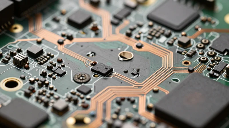
Defining Substrate-Like PCB (SLP) Architecture
Substrate-Like PCB (SLP) represents a significant leap in circuit board fabrication, specifically designed to overcome the density limitations of traditional High-Density Interconnect (HDI) methods. By utilizing mSAP (modified Semi-Additive Process) manufacturing techniques—commonly used in IC substrate production—SLP allows for line widths and spacing below 30 micrometers. This architectural shift enables AR/VR manufacturers to pack more processing power and signal integrity into a smaller footprint, essential for achieving the high-resolution, low-latency performance required for immersive experiences.
Comparative Analysis: HDI vs. SLP
| Feature | Standard HDI | SLP (mSAP) |
|---|---|---|
| Min. Line Width/Space | 40-50 µm | <30 µm |
| Fabrication Process | Subtractive | Modified Semi-Additive (mSAP) |
| Signal Integrity | Moderate | High (Reduced Impedance) |
| Component Density | Standard | Ultra-High |
The Semiconductor-Board Hybrid Model
The primary innovation in SLP technology is the adoption of semiconductor packaging standards for PCB manufacturing. While traditional boards use a subtractive etching process that often results in irregular trace sidewalls and signal loss, mSAP builds circuitry layer-by-layer through plating. This results in precise, vertical-walled traces that minimize skin effect losses—a critical factor when driving high-frequency data streams to 8K micro-OLED displays in head-mounted displays. By effectively turning the PCB into an IC-grade substrate, engineers can integrate complex System-on-Chips (SoCs) and memory modules closer together, drastically reducing board area.
Frequently Asked Questions
- Why does SLP matter for AR/VR head-mounted displays?
As headsets move toward lightweight, glasses-like form factors, every millimeter of internal space is critical. SLP allows for miniaturization of the motherboard, providing room for larger battery capacities and improved cooling solutions. - Does SLP increase the thermal load on AR/VR devices?
While SLP increases component density, it also enables more efficient trace routing and shorter path lengths. By reducing the overall circuit surface area, it can help optimize power distribution and minimize thermal buildup associated with long, resistive trace paths. - Is SLP compatible with standard surface mount technology?
Yes, SLP is compatible with existing SMT lines, though the fine-pitch requirements necessitate more advanced precision during pick-and-place and reflow soldering processes.
Material Science: The Hunt for Low-Loss Dielectrics
The Dielectric Challenge in Immersive Optics
As AR/VR headsets evolve toward 8K-per-eye resolutions and sub-10ms motion-to-photon latency, traditional PCB materials are reaching their physical limits. The primary barrier is the dissipation factor (Df) and dielectric constant (Dk) of standard FR-4 laminates. At high gigahertz frequencies, signal energy is lost as heat within the dielectric material, leading to significant signal degradation and jitter. Next-generation headsets require substrates that maintain electrical stability and low signal loss despite the thermal constraints inherent in compact, wearable form factors.
Material Comparison: Traditional vs. Next-Gen Laminates
| Material Category | Dielectric Constant (Dk) | Dissipation Factor (Df) | Target Application |
|---|---|---|---|
| Standard FR-4 | 4.4 - 4.8 | 0.020 | Basic logic/power |
| Modified Polyimide | 3.2 - 3.5 | 0.005 | High-speed flex/rigid-flex |
| PTFE-Based Laminates | 2.1 - 2.5 | 0.001 | RF/mmWave front-end |
| LCP (Liquid Crystal Polymer) | 2.9 - 3.0 | 0.002 | Ultra-miniature, high-freq |
Key Material Innovations
Engineers are increasingly turning to PTFE-based (Polytetrafluoroethylene) composites and LCP (Liquid Crystal Polymer) substrates. PTFE-based materials offer exceptional electrical stability, making them the gold standard for high-frequency RF transmission. However, their physical processing is notoriously difficult, often requiring specialized surface preparation. Alternatively, Modified Polyimide provides a pragmatic middle ground, offering improved thermal resistance and mechanical flexibility with significantly lower dielectric loss than standard polyimide, making it ideal for the complex folding patterns required in modern headsets.
Material Selection FAQ
- Why is the dissipation factor (Df) critical for AR/VR?
A high Df causes signal attenuation. In AR/VR, even minor signal loss can trigger synchronization errors in high-bandwidth video streams, leading to screen tearing or perceived motion lag. - Is PTFE suitable for all layers of a high-end VR headset?
While superior in electrical performance, PTFE is costly and difficult to manufacture in multi-layer stackups; it is typically reserved for high-speed signal layers while more robust, cost-effective materials are used for power and ground planes. - How does moisture absorption impact dielectric performance?
Moisture ingress significantly increases the effective Dk and Df of a board. Advanced materials like LCP offer near-zero moisture absorption, ensuring performance consistency across different environmental humidity conditions.
Mitigating Latency through Optimized PCB Routing

Precision Length Matching for Synchronous Data Flow
In high-speed VR optical engines, data streams must arrive simultaneously to prevent frame tearing and motion-to-photon latency. Length matching—the process of equalizing the physical length of differential pairs—is critical. Even microscopic disparities in trace length introduce phase shifts in high-speed signaling, leading to jitter that degrades visual fidelity. Engineers must employ advanced serpentining techniques, utilizing arc-based routing to prevent sharp corners that trigger impedance discontinuities and unwanted electromagnetic interference (EMI).
Controlling Trace Impedance at Multi-GHz Frequencies
Maintaining controlled impedance is the foundation of signal integrity in AR/VR headsets. As data rates climb into the multi-gigabit range, PCB traces act as transmission lines where impedance mismatches result in signal reflections. Achieving a consistent 50-ohm single-ended or 100-ohm differential impedance requires tight tolerance control over dielectric thickness, trace geometry, and copper roughness.
| Design Factor | Impact on Latency | Optimization Strategy |
|---|---|---|
| Trace Geometry | Reflections/Signal Loss | Use laser direct imaging (LDI) for sub-mil tolerances. |
| Dielectric Constant (Dk) | Propagation Velocity | Use PTFE-based materials for uniform Dk across frequencies. |
| Copper Roughness | Skin Effect/Attenuation | Specify VLP (Very Low Profile) copper foils. |
Best Practices for Real-Time Optical Engine Routing
- How does via stitching affect high-speed signals?
Improperly placed vias act as capacitive loads; using back-drilling to remove via stubs is essential to prevent signal reflection at high frequencies. - Why is reference plane continuity critical?
A fractured reference plane forces return currents to take long, inductive paths, drastically increasing loop area and EMI while degrading timing margins. - What role does crosstalk mitigation play?
By increasing inter-pair spacing to at least 3x the trace width, engineers can significantly reduce electromagnetic coupling between high-density signal lanes.
import math

def calculate_propagation_delay(l, er):
    # Speed of light in vacuum = 299.79 mm/ns
    # v = c / sqrt(er)
    velocity = 299.79 / math.sqrt(er)
    return l / velocity

# Example for 50mm trace on FR-4 (er ~ 4.4)
print(f'Latency: {calculate_propagation_delay(50, 4.4):.4f} ns')
Thermal Management Challenges in Ultra-Compact Form Factors
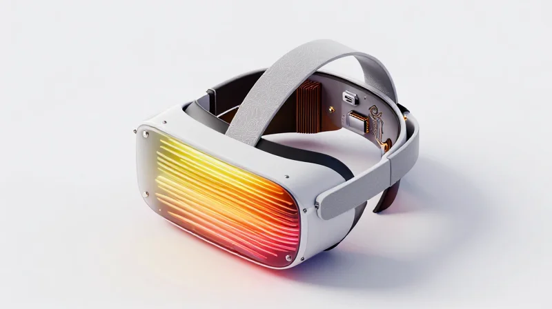
Managing Heat Density in AR/VR Architectures
In the confined chassis of modern AR smart glasses and VR headsets, heat density has become the primary bottleneck for sustained high-fidelity performance. As PCBs shrink to accommodate sophisticated optical engines and high-resolution displays, the concentration of thermal energy increases exponentially. Effective thermal management requires a multi-layered approach that integrates passive heat spreading, optimized PCB layer stack-ups, and conductive thermal pathways, ensuring that silicon stays within optimal operating temperatures to avoid thermal throttling during intensive processing tasks.
Integrated Thermal Dissipation Techniques
Engineers are moving beyond traditional heat sinks to utilize the PCB itself as a vital thermal conduit. Techniques such as high-density micro-via arrays act as thermal vias, pulling heat from surface-mounted SoCs directly into internal ground planes. This turns the multilayer PCB into a distributed heat spreader, effectively lowering the junction temperature of sensitive components.
| Technique | Mechanism | Primary Benefit |
|---|---|---|
| Thermal Vias | Conductive copper columns | Lowers thermal resistance to ground |
| Embedded Heat Spreaders | Copper foil layers/inlays | Lateral heat distribution |
| Phase Change Materials | Thermal interface transition | Efficient transient heat absorption |
Thermal Management FAQ
- Why does thermal throttling occur in ultra-compact VR hardware?
Thermal throttling occurs when internal components reach safety thresholds; the SoC reduces its clock speed to prevent permanent hardware damage, leading to dropped frames and perceived latency. - How do PCB materials influence thermal regulation?
High-Tg (glass transition temperature) laminates are essential in high-density designs to maintain mechanical stability and electrical integrity under the prolonged heat cycles inherent in AR rendering. - What is the role of ground planes in thermal design?
Beyond signal integrity, copper ground planes serve as massive heat sinks; proper copper pouring and strategic placement ensure that heat is diverted away from the processing core toward the chassis or external housing.
Strategic Considerations for Scaling AR/VR Manufacturing
The Economics of Advanced Interconnects
Transitioning from traditional FR-4 materials to advanced substrates like mPI (modified Polyimide) or PTFE-based laminates introduces significant cost volatility. While these materials are essential for achieving the low-loss, high-speed signals required for 8K-per-eye resolutions, they command a premium price and require specialized handling during the manufacturing process. Manufacturers must evaluate the Total Cost of Ownership (TCO) by factoring in not just material costs, but the long-term benefit of reducing thermal throttling and signal degradation, which directly correlates to device longevity and user retention.
Supply Chain Readiness and Yield Management
| Metric | Standard PCB (FR-4) | Advanced HDI/mPI | Strategic Impact |
|---|---|---|---|
| Manufacturing Complexity | Low | High | Requires specialized vendor partners |
| Typical Yield Rate | 98%+ | 85% - 92% | Higher waste necessitates buffering |
| Lead Time | 2-4 weeks | 8-14 weeks | Requires forward-looking procurement |
Key Considerations for Scaling Production
- How do I mitigate yield risks with high-density designs?
Implement early-stage Design for Manufacturing (DFM) audits and establish redundant fabrication partnerships to ensure output consistency despite complex layer stack-ups. - Is the supply chain ready for advanced substrates?
While specialized, capacity is growing. Manufacturers should prioritize long-term agreements with vendors who have mastered the registration accuracy required for fine-pitch HDI routing. - How does PCB selection affect time-to-market?
Opting for cutting-edge materials may extend prototyping cycles, but it significantly reduces the likelihood of late-stage hardware redesigns necessitated by thermal or signal integrity failures.
As the industry races toward more powerful spatial computing platforms, the choice of interconnect technology remains the decisive factor between consumer success and hardware stagnation. Whether leveraging the flexibility of rigid-flex or the precision of SLP, engineering teams must prioritize signal integrity and miniaturization to meet tomorrow’s immersive standards. Contact our lead engineering consultants today to discuss optimizing your PCB architecture for your next generation of AR/VR hardware.
