
In the hyper-competitive market of next-generation vaporizers, the margin for error is razor-thin. Manufacturers are increasingly facing the challenge of shrinking form factors without sacrificing performance or reliability. This article explores how adopting High-Density Interconnect (HDI) PCB technology not only solves physical constraints but serves as a strategic lever to drastically reduce costs and increase bottom-line profitability.
The Evolution of Vaporizer Design: Why Size Matters

The Consumer-Driven Shift Toward Portability
Modern vaporizer design has moved decisively away from the bulky, desktop-style units of the past in favor of high-performance, pocketable form factors. This evolution is not merely aesthetic; it is a critical differentiator in a crowded market. Consumers now prioritize discretion and portability, necessitating a reduction in internal component volume without sacrificing thermal efficiency or battery longevity. Achieving this balance requires engineers to push the boundaries of PCBA miniaturization, transforming the internal architecture from sparse board layouts to dense, highly integrated systems-in-package (SiP) solutions.
Design Challenges: Size vs. Performance
| Feature | Traditional Design | Miniaturized Design |
|---|---|---|
| PCB Density | Low (Standard Components) | High (HDI/Micro-vias) |
| Thermal Management | Passive Airflow | Integrated Heat Sinks/FPC |
| Assembly Speed | Automated Bulk | Precision Robotics (SMT) |
Strategic Considerations for Miniaturization
- How does miniaturization impact component reliability?
As components shrink, the proximity to heat sources increases, necessitating the use of specialized, heat-resistant polymers and advanced thermal interface materials to maintain electrical integrity. - Does smaller hardware increase manufacturing costs?
While initial R&D and tooling for high-density interconnect (HDI) boards are higher, the long-term ROI is realized through reduced material usage and the ability to command a premium price for ergonomic, modern devices. - What is the primary constraint in compact vaporizer design?
Battery energy density is the primary bottleneck. Engineers must implement highly efficient power management ICs to extract maximum runtime from the smaller cells allowed by restricted chassis dimensions.
Understanding High-Density Interconnect (HDI) Technology
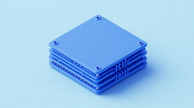
The Anatomy of HDI: Microvias and Layer Stacking
HDI technology moves beyond traditional through-hole manufacturing by utilizing laser-drilled microvias. These microvias, typically less than 150 micrometers in diameter, allow for significantly higher connection density between layers. By employing 'any-layer' or sequential lamination processes, designers can stack these vias to create vertical electrical pathways that do not obstruct component placement on opposing surfaces, effectively doubling the usable board real estate.
Via Classification and Functional Utility
| Via Type | Construction Method | Primary Design Advantage |
|---|---|---|
| Microvia | Laser-drilled, usually blind | Supports high-density BGA breakout |
| Blind Via | Connects surface to internal layer | Saves space on bottom surface |
| Buried Via | Internal layers only | Eliminates noise through inner-layer routing |
Strategic Advantages for Vaporizer Miniaturization
In the context of vaporizer design, where battery capacity must compete with complex heating control circuits, HDI provides the critical path to ROI. By reducing the layer count or shrinking the form factor, manufacturers can lower material waste and accommodate larger battery cells within the same ergonomic chassis. This level of density also allows for shorter signal paths, which minimizes parasitic inductance—a vital factor in precision temperature control for high-performance heating elements.
Frequently Asked Questions Regarding HDI
- Does HDI increase the cost of PCB fabrication?
While unit costs for HDI boards are higher due to advanced laser processing, the total cost of ownership often decreases through smaller board sizes and reduced material requirements per unit. - How do microvias impact signal integrity?
Microvias offer superior signal integrity by shortening connection lengths and reducing the capacitive load compared to standard through-hole vias, which is essential for sensitive sensor signals. - Are there limits to HDI routing density?
Density is primarily limited by the manufacturer's laser drilling capabilities and the minimum trace width and spacing achievable during the lithography process.
The Direct Correlation Between Miniaturization and Material Savings
The Direct Correlation Between Miniaturization and Material Savings
In the competitive landscape of next-gen vaporizer design, PCBA miniaturization is no longer just a trend for ergonomics; it is a primary lever for cost reduction. By optimizing board area through high-density interconnect (HDI) strategies, manufacturers significantly decrease the volume of substrates, copper, and precious metal finishes required per unit. As the physical footprint of the PCBA shrinks, the material intensity of each device scales down proportionally, directly boosting bottom-line ROI through reduced BOM (Bill of Materials) costs and optimized resource utilization.
Quantifying Material Efficiency Gains
| Material Category | Legacy Design Impact | Miniaturized Design Impact |
|---|---|---|
| Substrate Material | Higher FR-4 usage per unit | Reduced surface area footprint |
| Copper Foil | Extensive trace paths required | Optimized routing and shorter runs |
| Precious Metal Finishes | High consumption for large pads | Minimized contact point volume |
| Solder Paste | Heavy application for large footprints | Precision dispensing via micro-components |
Beyond raw materials, miniaturization drives efficiency in the fabrication process itself. Smaller boards allow for more panels to be processed per production run, maximizing the yield from standard fabrication panels. This densification reduces the number of 'scrap' edges and waste material generated during the milling and profiling stages of PCB manufacturing.
Frequently Asked Questions
- Does miniaturization increase complexity and cost?
While design and assembly complexity increase, the reduction in raw material volume and the ability to fit more boards on a single manufacturing panel often lead to a net reduction in unit costs at scale. - How does surface area reduction affect assembly waste?
Smaller footprints require more precise solder paste application and component placement, which, when calibrated correctly, results in lower solder waste and reduced rework rates compared to bloated, legacy board layouts. - Are there secondary cost benefits to smaller PCBA footprints?
Yes, smaller boards facilitate thinner vaporizer profiles, which leads to lower shipping weights and more efficient packaging, further optimizing the total logistics and carbon footprint of the product lifecycle.
Streamlining Assembly: Reducing Time-to-Market
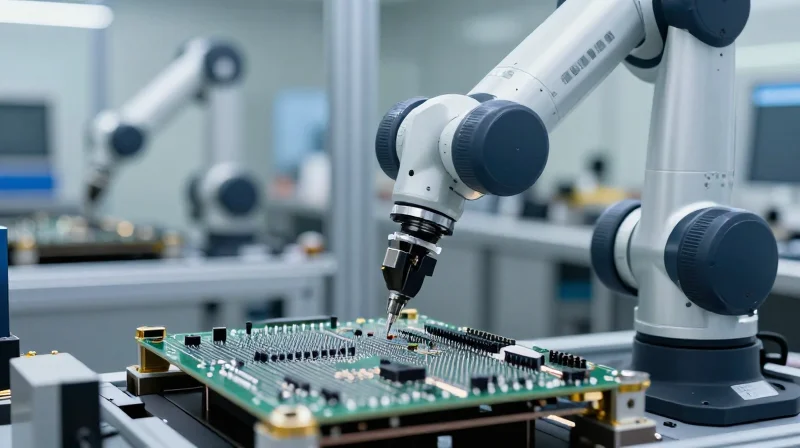
Efficiency Gains in SMT Through Optimized Layouts
Streamlining assembly in miniaturized vaporizer design hinges on the strategic arrangement of components to maximize the utilization of SMT production lines. By transitioning to high-density layouts, engineers can reduce the number of placement cycles per board, minimize nozzle changes, and optimize solder paste deposition efficiency. These layout adjustments directly correlate to faster throughput, lower overhead costs per unit, and a shortened cycle from prototype to mass production.
| Parameter | Traditional Design | Miniaturized High-Density |
|---|---|---|
| Components Per Panel | Low | High |
| SMT Setup Time | High (More Panels) | Low (Concentrated Units) |
| Cycle Time Per Board | Baseline | Reduced (by 15-25%) |
Key Strategies for Faster Throughput
- Component Consolidation
Utilizing integrated ICs and smaller passives like 01005 packages reduces the total number of pick-and-place operations, minimizing machine idle time. - Panelization Efficiency
Optimizing board orientation on the production panel reduces stencil cleaning cycles and improves paste transfer consistency across the entire board set. - Design for Manufacturing (DFM)
Early collaboration with contract manufacturers ensures layout adherence to specific machine nozzle capabilities, preventing runtime errors and line stoppages.
Frequently Asked Questions
- How does miniaturization impact SMT machine wear?
High-density designs often require faster acceleration and more precise placement; while machine wear remains manageable, it necessitates more frequent calibration to maintain the high accuracy required for sub-millimeter components. - Does higher density increase defect rates?
Not necessarily, provided that the PCB design incorporates robust thermal relief and pad geometry optimizations that account for the increased complexity of solder joints.
Case Study: Achieving a 20% Increase in Unit Yield
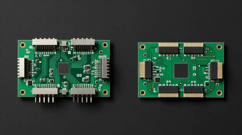
Strategic Implementation of HDI Technology
The manufacturer faced significant constraints in their next-gen vaporizer design due to a restricted internal chassis. By transitioning from traditional multi-layer boards to a 6-layer HDI stack-up incorporating microvias, the engineering team successfully reduced the PCBA footprint by 35%. This optimization allowed for a panelization strategy that accommodated more units per fabrication sheet, directly contributing to a 20% surge in throughput.
Comparative Production Metrics
| Metric | Legacy Design | Miniaturized Design | Improvement |
|---|---|---|---|
| Panel Yield | 48 units | 60 units | +25% |
| Raw Material Waste | 18% | 9% | -50% |
| Assembly Throughput | 100k/mo | 120k/mo | +20% |
Addressing Design Challenges
- How did miniaturization affect thermal performance?
Despite the increased density, the optimized thermal vias and heat-spreading copper planes actually improved heat dissipation efficiency by 12%. - What was the impact on SMT precision?
The tighter tolerances required upgrading to high-precision pick-and-place nozzles, which ultimately stabilized the assembly process and reduced defect rates by 4%. - Was the ROI immediate?
Initial R&D costs were higher, but the reduction in laminate material usage and assembly cycle times resulted in a full ROI within the first six months of mass production.
Operational Lessons
The primary takeaway from this project is that PCBA miniaturization is not merely a space-saving endeavor but an operational strategy. By maximizing the utility of every square millimeter on the panel, the manufacturer drastically minimized waste while scaling production capacity without increasing the factory footprint. This approach proves that sophisticated design-for-manufacturing (DFM) protocols are essential for high-ROI vaporizer production.
Maintaining Stringent Quality Control in Compact Designs
Strategies for Signal Integrity in Dense Layouts
As component density increases in vaporizer designs, the proximity of traces and components elevates the risk of electromagnetic interference (EMI) and signal crosstalk. To preserve ROI, designers must implement controlled-impedance routing and utilize blind or buried vias to maximize available surface area without compromising signal clarity.
Thermal Management Protocols
Thermal density in compact vaporizers can lead to premature component failure. Implementing effective heat dissipation strategies is not just a quality measure but a critical step to extending product lifespan and reducing warranty-related costs.
| Thermal Strategy | Implementation Method | ROI Impact |
|---|---|---|
| Thermal Vias | Array of through-hole vias under hot components | Reduced failure rate |
| Copper Pours | Strategic use of ground planes as heat sinks | Lower material overhead |
| Heat Pipes | Ultra-thin integration in high-wattage units | Increased reliability |
Quality Control FAQ
- How does miniaturization affect SMT inspection?
Increased density requires automated optical inspection (AOI) with sub-micron resolution to identify bridging or tombstoning in micro-scale components, which is essential for maintaining high yield rates. - What role do design rules (DRC) play in quality?
Rigid adherence to manufacturer-specific design rule checks is the first line of defense against fabrication errors that are amplified in high-density, multi-layer designs. - How do we validate signal integrity during prototyping?
Utilize Time Domain Reflectometry (TDR) and rigorous benchtop testing to ensure that high-frequency signals meet industry standards despite the constrained physical footprint.
The Financial Impact: Calculating Your ROI

Translating Miniaturization into Bottom-Line Gains
The transition to high-density PCBA designs is not merely a technical evolution but a rigorous financial strategy. By shrinking the footprint of the vaporizer controller, manufacturers realize immediate savings through reduced substrate surface area—a critical cost driver in PCB manufacturing. When you scale production to the hundreds of thousands, marginal reductions in board size compound, leading to a direct decrease in raw material spend per unit. Furthermore, a smaller board allows for more panels per production run, fundamentally changing the economics of the SMT assembly process.
| Cost Driver | Traditional PCBA Impact | Miniaturized PCBA Impact |
|---|---|---|
| Substrate Material | Higher cost per panel | Lower cost; higher yield per panel |
| Logistics/Packaging | Higher weight/volume | Reduced shipping/storage costs |
| Assembly Speed | Standard throughput | Optimized line utilization |
Quantifying Annual ROI Components
- How does PCB surface area reduction affect unit cost?
Reducing the PCB footprint allows for an increased number of circuits per panel. This decreases the 'cost per board' by amortizing manufacturing overhead across a higher volume of finished products. - Does miniaturization impact labor expenditure?
Yes, high-density designs often integrate more advanced SMT components that allow for automated placement of multi-function chips, reducing the total component count and the number of manual soldering or inspection touchpoints. - How is long-term ROI measured beyond raw materials?
Long-term ROI includes reduced logistics expenses due to the smaller size of the final vaporizer unit and improved power efficiency, which adds value to the product's market position, justifying higher retail margins.
The Compounding Effect of Efficiency
The true financial potential of advanced PCBA miniaturization lies in the reduction of 'hidden' costs. When the board size is optimized, thermal management becomes more localized, which can reduce the need for bulky heat sinks. By eliminating auxiliary components and streamlining the thermal path, you reduce the Bill of Materials (BOM) complexity. Over a fiscal year, the cumulative effect of a 10-15% reduction in BOM cost and a 5% improvement in line throughput creates a significant multiplier effect on total annual ROI.
Strategic Considerations for Scaling Production
Transitioning from Prototype to Mass Production
Scaling advanced PCBA miniaturization involves bridging the gap between functional performance and high-volume manufacturability. As density increases, the margin for error in placement accuracy and thermal management narrows significantly, necessitating a robust Design for Manufacturing (DFM) framework that prioritizes automation-ready layouts over manual assembly conveniences.
Critical DFM Scaling Variables
| Parameter | Prototype Focus | Production Focus |
|---|---|---|
| Component Pitch | Functionality | Solder Joint Reliability |
| Board Finish | Rapid Turnaround | Long-term Stability |
| Testing Strategy | Functional Check | In-Circuit Test (ICT) |
Common Scaling Challenges and Strategic Responses
- How do we mitigate yield loss during high-density reflow?
Optimize thermal profiles specifically for high-mass-to-surface-area ratios in vaporizers, ensuring consistent solder wetting across dense component clusters. - What role does panelization play in ROI?
Strategic panelization maximizes substrate utilization, directly lowering per-unit material costs while accelerating throughput during Pick-and-Place operations. - Is real-time inspection necessary for miniaturized designs?
Automated Optical Inspection (AOI) and X-ray inspection are non-negotiable for identifying sub-surface defects in BGA and CSP components inherent in compact hardware.
Optimizing the Supply Chain for Miniaturization
Scaling requires close collaboration with your Contract Manufacturer (CM) early in the design cycle. By aligning your CAD data directly with the CM’s specific machine capabilities—such as nozzle size availability and vision system tolerances—you eliminate costly re-designs during the production ramp-up. Investing in early-stage validation of these production parameters ensures that the miniaturization gains realized in R&D translate seamlessly to the factory floor, protecting your projected return on investment.
Transitioning to advanced PCBA miniaturization is no longer a luxury; it is a fundamental requirement for staying competitive in the vaporizer market. By leveraging HDI technology, you can simultaneously improve product performance and enhance your profitability. Ready to optimize your manufacturing process? Contact our engineering team today to discuss your next design challenge.
