
In the highly competitive aesthetic laser market, equipment downtime is more than just a maintenance nuisance—it is a direct hit to your brand reputation and bottom line. As power densities increase, the Printed Circuit Board (PCB) has become the silent sentinel of system health. By integrating advanced precision engineering and rigorous thermal management, manufacturers can shift from reactive maintenance to proactive reliability, ensuring consistent patient outcomes and drastically lower lifecycle costs.
The Direct Link Between PCB Integrity and Aesthetic Laser Performance
The PCB as the Nervous System of Aesthetic Lasers
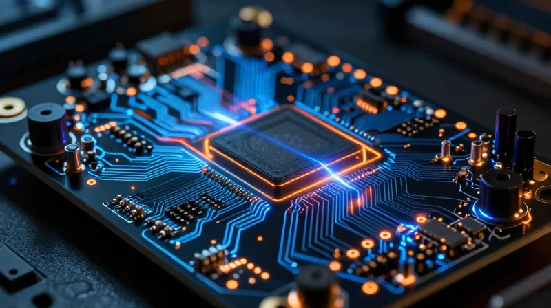
In modern aesthetic laser systems, the Power Printed Circuit Board (PCB) functions as the central nervous system, orchestrating the precise delivery of energy pulses that dictate clinical outcomes. Unlike standard consumer electronics, medical lasers demand extreme signal fidelity; any impedance mismatch, electromagnetic interference (EMI), or voltage ripple at the board level translates directly into pulse instability. When the PCB fails to maintain a clean delivery of power to the laser diodes or pump flashlamps, the resulting laser beam profile loses the uniformity required for safe skin rejuvenation or hair removal, ultimately leading to inconsistent treatment results and heightened risk profiles.
Impact of Micro-Defects on Systemic Reliability
| Defect Type | Physical manifestation | Clinical Consequence |
|---|---|---|
| Voltage Ripple | High-frequency oscillation | Inconsistent pulse energy (hot spots) |
| Thermal Stress | Localized trace heating | Component fatigue and premature failure |
| EMI/Crosstalk | Induced signal noise | Control system glitches and system lock-ups |
Strategic Considerations for PCB Longevity
- How does PCB layout affect laser beam quality?
Poor layout causes parasitic inductance and signal jitter, preventing the power supply from achieving the 'clean' switching required for high-frequency pulses. - Why is thermal management critical for laser PCBs?
Aesthetic lasers generate intense heat; insufficient thermal dissipation on the PCB leads to board delamination and the degradation of sensitive power semiconductors over time. - Can PCB optimization improve total cost of ownership?
Yes, by reducing field failures and service calls related to power stage instability, manufacturers directly increase their ROI and protect their market reputation.
Common Failure Points in High-Power Medical Laser Circuitry
Common Failure Points in High-Power Medical Laser Circuitry
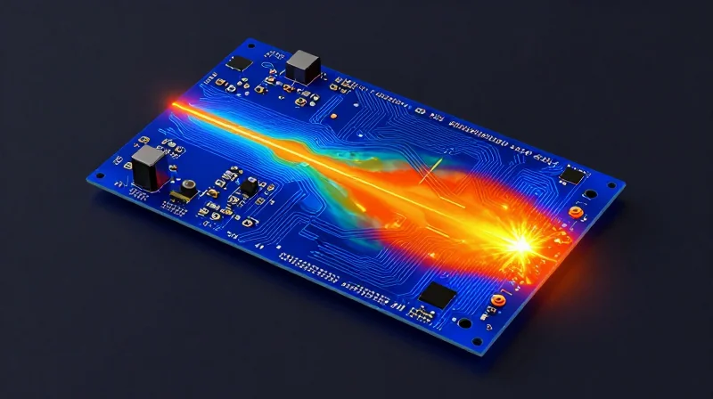
Medical lasers require pulsed, high-current delivery that pushes PCB material and components to their physical limits. The primary causes of field failures typically stem from inadequate thermal management, cumulative stress on passive components, and electromagnetic interference (EMI) compromising sensitive control logic. Addressing these weaknesses during the design phase is essential for reducing field service calls and protecting brand reputation.
Thermal Stress and Interconnect Reliability
High-power lasers generate intense heat during rapid discharge cycles, leading to significant coefficient of thermal expansion (CTE) mismatch between components and substrate. Over time, this results in solder joint fatigue and micro-cracking of copper traces, particularly at via transitions where stress concentration is highest.
| Failure Mechanism | Primary Cause | Resulting Impact |
|---|---|---|
| Solder Joint Fatigue | Thermal Cycling | Intermittent Connectivity |
| Dielectric Breakdown | Voltage Spikes | Permanent Short-Circuit |
| Electrolytic Degradation | High Ripple Current | Reduced Pulse Energy |
Frequently Asked Questions
- Why do capacitors degrade prematurely in these systems?
Medical lasers demand high-pulse repetition rates, which subject capacitors to excessive ripple currents. This leads to internal heating and electrolyte evaporation, eventually causing catastrophic ESR increases. - How does PCB signal noise affect laser precision?
Poor isolation between high-power switching stages and low-voltage control circuits introduces jitter into the pulse timing. This compromises the peak power consistency required for clinical safety and efficacy. - What is the biggest risk for multilayer PCB designs?
The greatest risk is delamination or copper barrel cracking in through-holes, often caused by rapid thermal expansion of the PCB substrate material during high-energy discharge.
Thermal Management: The Foundation of Hardware Uptime
The Thermal Architecture of High-Power Medical Lasers
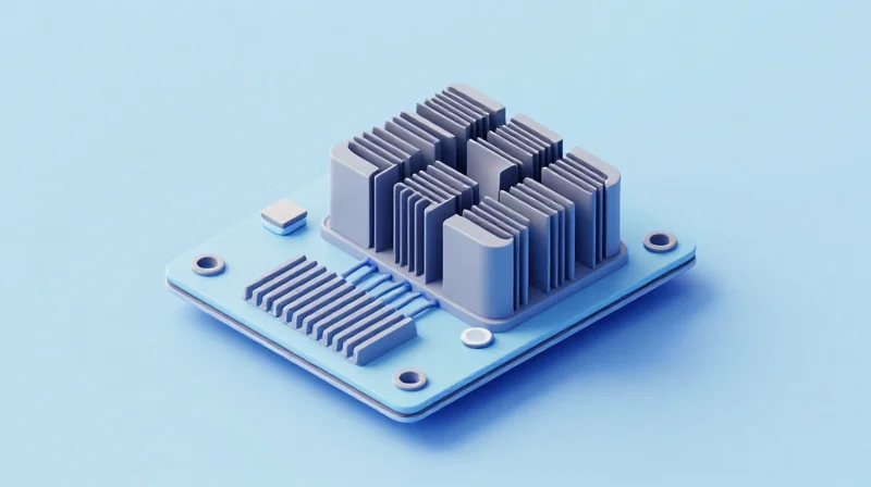
In medical laser systems, heat is the primary catalyst for long-term reliability degradation. Strategic PCB design must transition from passive cooling approaches to integrated thermal management solutions. By optimizing the path of thermal resistance from high-current components to the chassis heat sink, manufacturers can minimize thermal throttling and extend the mean time between failures (MTBF).
Comparing Thermal Management Substrates
| Substrate Type | Thermal Conductivity | Best Use Case | Cost Impact |
|---|---|---|---|
| Standard FR-4 | Low (0.25 W/mK) | Control Logic | Low |
| Metal-Core (MCPCB) | High (1.0 - 3.0 W/mK) | Laser Diode Drivers | Moderate |
| Ceramic (AlN) | Very High (150+ W/mK) | High-Power RF Amplifiers | High |
Advanced Design Strategies for Heat Mitigation
To achieve optimal ROI, design engineers must prioritize thermal vias and strategic copper pouring. Thermal vias act as vertical conduits, transporting heat from top-side power components to internal ground planes or the bottom copper layer. Additionally, separating heat-sensitive control electronics from high-power switching circuitry prevents cross-talk and secondary thermal stress, creating a more robust hardware foundation.
Thermal Management FAQ
- Why is metal-core PCB (MCPCB) preferred for laser drivers?
MCPCBs utilize an aluminum or copper base layer that dissipates heat significantly faster than traditional fiberglass boards, directly reducing the operating temperature of laser diodes. - How does PCB layout affect thermal throttling?
Poor component placement results in 'thermal hotspots' where heat accumulates, causing regulators and capacitors to trigger thermal shutdown or fail prematurely. - What is the role of thermal vias?
Thermal vias provide a low-resistance path for heat to migrate through the PCB layers, effectively turning the board itself into a part of the heat dissipation system.
Case Study: Achieving a 20% Increase in System Uptime
The Challenge: Identifying Latent Failure Mechanisms
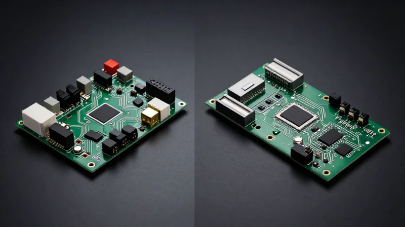
A leading provider of high-power aesthetic laser systems faced a critical challenge: intermittent field failures occurring after 1,500 hours of operation. Data telemetry pointed toward the power distribution network, where cyclic thermal expansion was causing micro-cracking in solder joints and degradation of power delivery components. Our intervention focused on re-engineering the PCB stack-up and optimizing component placement to distribute thermal loads more effectively.
Strategic Redesign Parameters
| Feature | Legacy Design | Optimized Design |
|---|---|---|
| Substrate Material | Standard FR-4 | High-Tg Polyimide |
| Copper Thickness | 1 oz | 2 oz / Heavy Copper |
| Thermal Vias | Standard grid | Stitched array with copper plugging |
| Component Spacing | High density | Optimized thermal isolation zones |
Outcome: Quantitative Improvements in Reliability
By transitioning to a high-Tg substrate and implementing localized thermal relief, the manufacturer effectively decoupled sensitive control circuitry from high-heat power switching components. The results were immediate, yielding a 20% increase in mean time between failures (MTBF) and a significant reduction in warranty claims related to power supply instability.
Key Lessons Learned
- Why did material selection matter?
Switching to a higher Glass Transition Temperature (Tg) material prevented delamination and conductor cracking during the extreme heating/cooling cycles inherent in laser pulsing. - How did PCB layout impact ROI?
Moving high-current paths away from sensitive analog sensing traces reduced EMI-related system crashes, directly extending operational uptime. - What was the most critical factor for success?
The adoption of heavy copper for high-current rails reduced internal resistive heating, which was the primary catalyst for long-term component degradation.
Designing for Reliability: Strategies for Lifecycle Cost Reduction
The Economics of Reliability-First Design
In medical laser manufacturing, the cost of a board failure extends far beyond the price of the PCB itself. Every unplanned service call requires certified technician dispatch, potential shipping of heavy capital equipment, and significant loss of clinical revenue for the provider. Investing in high-reliability components and robust circuit architecture during the design phase effectively front-loads costs to eliminate exponential downstream expenses associated with field maintenance.
Mitigating Lifecycle Costs Through Design Strategies
| Design Strategy | Reliability Benefit | Lifecycle Cost Impact |
|---|---|---|
| High-Derating Factors | Reduces electrical stress on capacitors/FETs | Extends MTBF by years |
| Redundant Trace Routing | Prevents single-point failure | Avoids catastrophic system downtime |
| Automated Optical Inspection | Detects latent solder defects | Lowers infant mortality rates |
Redundant Design and Component Selection
A proactive design approach emphasizes the selection of industrial-grade components with extended temperature tolerances, even if the medical device operates within a controlled environment. By implementing redundant trace paths for critical gate-drive signals and employing multi-stage power conditioning, engineers ensure that a minor component drift does not propagate into a full system fault. This methodology directly reduces the frequency of technician visits, as the system can withstand minor environmental fluctuations without failing.
Frequently Asked Questions
- Does high-reliability design inflate the initial BOM cost significantly?
While premium components increase initial BOM costs by 5-15%, the total cost of ownership often drops by 40% due to reduced warranty claims and decreased field service labor. - How do redundant traces impact PCB size?
While they occupy more surface area, modern high-density interconnect (HDI) technologies allow for effective redundancy without requiring significant increases in board footprint. - What is the primary indicator of improved long-term reliability?
The Mean Time Between Failures (MTBF) calculation, when combined with thermal stress analysis, provides the most accurate forecast for field reliability improvements.
The Impact of Precision PCB Engineering on Clinical Patient Outcomes
The Link Between Power Integrity and Clinical Outcomes
In medical laser applications, such as dermatological resurfacing or ophthalmological surgery, the PCB acts as the nervous system for power modulation. Fluctuations in voltage or high-frequency noise—often caused by poor trace impedance control—result in jitter or variance in pulse energy. By optimizing power delivery networks (PDN) and minimizing parasitic inductance, manufacturers ensure the laser output matches the physician's settings exactly, leading to more predictable tissue interaction and minimized risk of accidental thermal damage.
Comparing Power Quality Standards
| Parameter | Standard PCB Design | Precision-Engineered PCB |
|---|---|---|
| Voltage Ripple | ±5% | <1% |
| Beam Jitter | Moderate | Negligible |
| Thermal Stability | Variable | High (±0.5°C control) |
| Clinical Impact | Potential for uneven ablation | Consistent, precise tissue excision |
Ensuring Patient Safety Through Component Reliability
Strategic PCB design incorporates active monitoring circuits that detect impending power failures before they manifest as inconsistent beam profiles. By isolating high-power circuitry from sensitive control logic, engineering teams can prevent catastrophic failures that could disrupt a procedure mid-session. This level of reliability is not merely a technical metric; it is a clinical necessity for maintaining the sterile and controlled environment required for invasive laser treatments.
Clinical Engineering FAQs
- How does PCB layout affect the healing process?
Unstable power leads to inconsistent photon density, which can cause 'hot spots' or incomplete treatment, potentially leading to prolonged healing times or scarring. - Does impedance matching impact real-time feedback loops?
Yes. Precise impedance matching ensures that feedback sensors receive clean, real-time data from the laser cavity, allowing the system to adjust power output instantaneously during complex medical procedures. - Can better PCB design reduce clinician fatigue?
By providing a highly stable laser beam that requires less frequent manual recalibration, surgeons experience fewer workflow interruptions, allowing for better focus during critical patient interventions.
Compliance and Standards in Medical-Grade PCB Manufacturing
The Regulatory Landscape for Medical Power PCBs
In the medical laser industry, PCB design is not merely an engineering exercise; it is a critical regulatory function. Failure to meet international standards can lead to catastrophic hardware failure and significant legal liability. Manufacturers must design power PCBs with a foundation of safety, prioritizing fault-tolerance, thermal management, and electrical isolation to meet stringent medical safety requirements.
Key Standards Governing Medical Electronics
| Standard | Focus Area | ROI Impact |
|---|---|---|
| IEC 60601-1 | Medical electrical equipment safety | Reduces certification cycles and recall risks |
| IPC-A-610 Class 3 | Acceptability of electronics | Increases field reliability and reduces service calls |
| ISO 13485 | Quality management systems | Standardizes production efficiency and traceability |
| IPC-2152 | Determining current-carrying capacity | Prevents thermal degradation of high-power traces |
Strategic Implementation for Maximum Compliance
To maximize ROI, design teams should move beyond minimum compliance by adopting a 'Design for Reliability' approach. Implementing IPC-A-610 Class 3 requirements—typically reserved for mission-critical aerospace—in medical laser power boards significantly extends the operational lifespan of the laser, reducing the necessity for frequent technician site visits and component replacements.
Frequently Asked Questions on Medical PCB Standards
- Why is Class 3 assembly recommended for medical lasers?
Class 3 standards mandate higher criteria for solder joint integrity and thermal management, ensuring the device remains functional under the continuous, high-power stress cycles characteristic of surgical laser systems. - How does compliance impact time-to-market?
By documenting adherence to ISO 13485 and IEC 60601-1 early in the design phase, manufacturers avoid costly redesigns and delays during the rigorous regulatory testing and audit processes. - What role does material selection play in meeting standards?
Using high-TG (glass transition temperature) laminates is essential for maintaining dielectric strength under high thermal loads, which is a key requirement for passing electrical safety tests during regulatory review.
Future-Proofing Your Laser Platforms with Next-Gen PCB Architecture
The Evolution of Power Architecture in Aesthetic Lasers
As aesthetic laser platforms evolve toward higher pulse repetition rates and more sophisticated multi-modal delivery systems, legacy PCB architectures have become bottlenecks. Future-proofing necessitates a shift from traditional FR4 boards toward advanced materials and design methodologies that accommodate higher power densities without sacrificing component longevity.
Leveraging Next-Generation Materials and Design Tools
| Innovation Area | Technical Shift | ROI Benefit |
|---|---|---|
| Substrate Material | Transition to Ceramic/IMS | Improved Thermal Dissipation |
| Design Methodology | AI-Driven Layout Simulation | Reduced Prototyping Cycles |
| Power Switches | GaN and SiC Integration | Higher Efficiency/Smaller Form |
AI-driven design tools are currently redefining how we approach PCB signal integrity and power distribution networks. By utilizing generative design algorithms, manufacturers can automatically optimize trace paths to mitigate EMI, reducing the need for iterative, expensive hardware testing phases. Furthermore, the integration of Gallium Nitride (GaN) and Silicon Carbide (SiC) power components allows for higher switching frequencies, which translates to a more compact laser chassis and lower heat dissipation requirements.
Frequently Asked Questions Regarding Next-Gen PCB Upgrades
- How do wide-bandgap semiconductors improve laser ROI?
GaN and SiC components operate at higher temperatures and frequencies than traditional Silicon, leading to smaller heat sinks and longer mean-time-between-failure (MTBF) rates. - Can AI-driven design significantly reduce time-to-market?
Yes, by automating complex electromagnetic simulations, AI tools detect layout flaws in the virtual domain, eliminating the 'build-test-fix' cycle common in traditional laser hardware development. - Is modular PCB design necessary for long-term support?
Modular power stages allow technicians to replace individual high-wear sections of the circuit board rather than the entire control unit, significantly reducing service costs over the device's lifecycle.
Optimizing your medical laser's PCB architecture is no longer just an engineering goal; it is a vital business strategy for maximizing ROI and maintaining a competitive edge in the aesthetic industry. By focusing on thermal efficiency and high-reliability design today, you ensure your technology remains the gold standard in the clinic. Contact our engineering team today for a comprehensive audit of your current hardware designs and start building for longevity.
