
Designing for high-performance medical aesthetic lasers presents unique engineering challenges. Balancing high-current pulse-width modulation with stringent regulatory safety standards requires a rigorous approach to Design for Manufacturing. In this guide, we break down the critical PCB design strategies to ensure your hardware is safe, reliable, and compliant.
The Intersection of High Power and Medical Precision
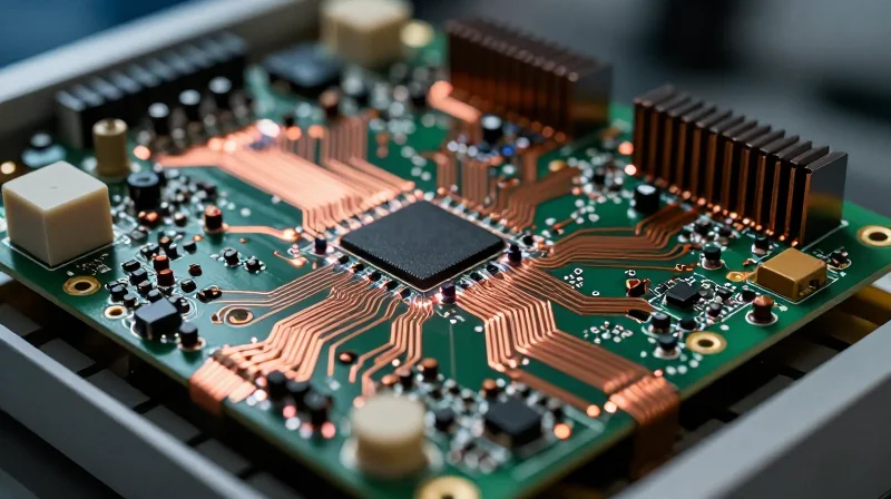
The Conflict: Power Density Versus Signal Integrity
In aesthetic laser hardware, the PCB must simultaneously manage high-current pulses—often exceeding tens of amperes—to drive flashlamps or diode arrays, while maintaining sub-microvolt precision for laser sensor feedback and calibration circuits. Standard industrial DFM guidelines often prioritize thermal dissipation or board footprint at the expense of electromagnetic compatibility (EMC). In a clinical laser environment, this approach is insufficient; high-current switching creates magnetic flux loops that can corrupt the high-impedance sensing paths required for skin-temperature monitoring and energy-dose verification.
Comparative DFM Requirements
| Requirement | Standard Industrial PCB | Medical Laser PCB |
|---|---|---|
| Current Handling | Trace width via IPC-2221 | Low-impedance planes + high-copper weight |
| EMI Mitigation | Basic grounding | Multi-layer isolation + tight return paths |
| Component Spacing | Minimal clearance | Creepage/Clearance per IEC 60601-1 |
| Reliability Focus | Cost/Time-to-market | Failure-mode redundancy/Long-term stability |
Critical DFM Considerations for Clinical Hardware
- Why does standard IPC-2221 trace sizing fail here?
Standard guidelines focus on trace temperature rise; however, they ignore the inductive effects of high-speed pulsing. In medical lasers, current loop area is more critical than trace resistance to avoid radiated emissions that cause erratic sensor behavior. - How does dielectric selection affect performance?
Standard FR-4 is often lossy under the high-frequency switching transients typical of modern aesthetic lasers. Utilizing higher glass transition temperature (Tg) materials is essential to prevent micro-cracking and impedance shifts during repeated clinical high-power cycles. - What is the primary risk of neglecting current return paths?
Improper return path design forces return currents to circulate through sensitive analog ground planes, inducing noise. This directly impacts the precision of energy delivery feedback, potentially leading to inconsistent treatment levels.
Designing for clinical-grade reliability demands a paradigm shift: treating the power stage and the control stage as a single, interdependent ecosystem. By integrating advanced DFM strategies—such as symmetrical stack-ups and strategic component partitioning—engineers can ensure that high-power delivery does not compromise the clinical efficacy and patient safety of the laser system.
Strategic Material Selection for Thermal Stability
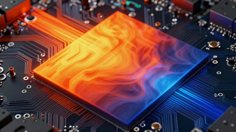
The Thermal Challenge in Aesthetic Laser Hardware
Medical aesthetic lasers subject PCBs to extreme thermal cycling caused by rapid, high-current pulses. Standard FR-4 laminates often succumb to delamination, copper barrel cracking, and dielectric breakdown under these conditions. Engineers must specify materials that offer high glass transition temperatures (Tg) to prevent the resin matrix from softening, which would otherwise lead to mechanical failure during thermal expansion.
Material Performance Comparison
| Parameter | Standard FR-4 | High-Tg Polyimide/Ceramic | Impact on Reliability |
|---|---|---|---|
| Tg (°C) | 130-140 | >200 | Higher Tg resists resin softening. |
| CTE Z-Axis | High (Unstable) | Low (Stable) | Prevents via-barrel fatigue. |
| Thermal Conductivity | Poor | Enhanced | Better heat dissipation. |
Best Practices for Material Selection
- Why is Tg selection critical for pulse-load hardware?
A high Tg ensures the board remains rigid above the operating temperature threshold, preventing the Z-axis expansion that frequently causes plated-through-hole (PTH) fractures in high-current applications. - Should I prioritize CTE (Coefficient of Thermal Expansion)?
Yes. Matching the CTE of the dielectric to the copper circuitry reduces stress at the interface, minimizing the risk of layer separation during rapid cooling and heating cycles characteristic of laser discharges. - What about CAF (Conductive Anodic Filament) resistance?
For medical-grade reliability, specify laminates with high CAF resistance to prevent electrical shorts between closely spaced vias that occur as moisture and heat degrade internal dielectric structures.
Copper Weight and Trace Geometry Optimization
In medical aesthetic laser systems, power delivery paths must maintain extreme signal integrity while facilitating high-current delivery for pulse-width modulation (PWM) stages. Under-dimensioning copper leads to resistive (I²R) losses, causing local heating that compromises sensitive nearby analog circuitry, while excessive copper can lead to parasitic capacitance that degrades switching performance. DFM optimization requires a precise balance between current capacity, thermal dissipation, and electromagnetic noise rejection.
Calculating Trace Widths for PWM Stability
When calculating trace dimensions for pulsed power, standard DC capacity charts often underestimate thermal accumulation. Designers must account for the Root Mean Square (RMS) current of the laser’s PWM cycle rather than peak current. To maintain thermal stability, aim for a temperature rise not exceeding 10°C over ambient, providing a safety margin for the confined environment of a laser handpiece or chassis.
| Parameter | Recommended Practice | Rationale |
|---|---|---|
| Copper Weight | 2 oz to 3 oz | Reduces DCR for high-current bursts |
| Trace Spacing | Greater than 20mil | Prevents HV arcing during peak transients |
| Via Stitching | Dense arrays | Distributes heat to inner layers |
DFM Considerations for High-Current Routing
- How does copper thickness affect thermal management?
Increased copper thickness lowers resistance, which reduces heat generation at the source, effectively turning the trace into a heat-spreading plane that protects the substrate from warping. - What is the danger of necking traces in power stages?
Any narrowing or 'necking' of high-current paths creates localized hot spots (bottlenecks) that can initiate PCB delamination and trigger voltage drops that manifest as power ripple in the laser output. - Why prioritize inner layer copper?
Utilizing internal layers for power distribution allows for balanced heat sinking across the PCB stack-up and provides a path for shielding, effectively isolating noise-sensitive logic.
Finally, ensure that all high-current traces are designed with rounded corners. Sharp 90-degree angles in heavy copper traces can act as stress risers during thermal cycling, potentially leading to copper cracking over the long operational life required by clinical-grade medical aesthetic equipment.
Advanced PWM Switching Noise Mitigation

In high-current laser systems, the rapid edge rates of PWM switching induce significant electromagnetic interference (EMI) and conducted emissions. Mitigating these transients requires a multi-layered approach combining tight loop-area management, strategic component placement, and advanced filtering techniques to protect low-noise analog control circuitry from power-stage coupling.
Routing Strategies for EMI Reduction
Minimizing loop inductance is the most effective defense against switching-induced noise. Designers must prioritize a 'current-return-path' philosophy, ensuring that high-current paths are strictly paired with low-impedance return planes directly underneath the trace to minimize the radiated loop area.
| Strategy | Effectiveness | Mechanism |
|---|---|---|
| Vertical Layer Stacking | High | Couples signal/return path closer to reduce loop inductance. |
| Stitched Ground Vias | Medium | Prevents impedance discontinuities at layer transitions. |
| Differential Signaling | High | Cancels out common-mode noise in sensitive sensor lines. |
Decoupling and Filtering Best Practices
- How does capacitor placement affect noise?
Decoupling capacitors must be placed as close as possible to the IC power pins to minimize parasitic inductance, which otherwise negates the capacitor's ability to shunt high-frequency switching noise. - Why use ferrite beads in power lines?
Ferrite beads act as high-frequency resistors, suppressing electromagnetic oscillations and preventing switching noise from traveling back onto the main DC supply rails. - Is bulk capacitance sufficient?
No; a hierarchical decoupling strategy utilizing high-frequency ceramics (low ESR/ESL) in parallel with bulk tantalum or polymer capacitors is necessary to cover both transient spikes and steady-state ripple.
Gate Drive Isolation
To prevent switching noise from the high-current MOSFET stage from contaminating the low-voltage logic (MCU), integrate galvanic isolation or high-speed optoisolators. This creates a physical barrier that prevents ground bounce from influencing delicate laser pulse timing and safety interlock circuits.
EMI Shielding and Regulatory Compliance
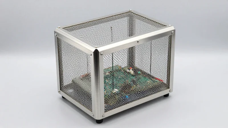
Strategies for EMI Containment in High-Current Laser Systems
High-current laser systems generate intense electromagnetic fields during discharge cycles that can interfere with sensitive control electronics and adjacent instrumentation. To meet IEC 60601-1-2 requirements, engineers must employ a multi-layered approach to electromagnetic compatibility (EMC). This involves aggressive board-level shielding (BLS), strategic use of ground planes, and effective partitioning of the noisy high-current paths from the low-voltage control signals.
Shielding Implementation Techniques
| Shielding Method | Primary Application | Compliance Impact |
|---|---|---|
| Board-Level Shielding (BLS) | Localized noise sources (PWM/FETs) | Reduces radiated emissions |
| Faraday Caging | Complete board enclosure | Enhances ESD and immunity |
| Stitched Via Fences | Edge of board/signal paths | Prevents common-mode emissions |
Regulatory Compliance and Validation
Compliance with medical standards such as IEC 60601-1-2 is not merely a post-design verification task but an iterative DFM process. Proactive simulation of magnetic coupling between high-current loops and sensitive analog inputs is critical to passing immunity testing.
- How does Faraday shielding protect laser medical hardware?
A well-designed Faraday cage prevents electromagnetic energy from radiating outside the system enclosure, ensuring the laser driver does not interfere with nearby life-critical diagnostic equipment. - Why is IEC 60601-1-2 compliance more difficult with high-current pulses?
The fast rise and fall times of PWM currents create high-frequency transients that possess high spectral content, making them prone to escaping via conduction or radiation. - What role does grounding play in EMC compliance?
Proper single-point or hybrid grounding prevents ground loops, which are common culprits in failing radiated immunity and emissions compliance tests for high-power devices.
Creepage and Clearance for Patient Safety
Defining Isolation Requirements
In medical aesthetic hardware, the distinction between creepage (shortest path along the surface of an insulator) and clearance (shortest path through air) is governed by IEC 60601-1 standards. For high-current laser drivers, inadequate spacing can lead to tracking—a conductive path forming across an insulating surface—especially in the humid environments often found in clinical settings.
DFM Strategies for Insulation Integrity
| Technique | Mechanism | Dfm Benefit |
|---|---|---|
| Slotting/Routing | Milling voids in PCB substrate | Increases creepage path length without board expansion |
| Conformal Coating | Applying dielectric barrier | Allows reduced clearance by mitigating airborne discharge |
| Track Shielding | Physical isolation barriers | Prevents dust buildup causing conductive bridges |
Frequently Asked Questions on Isolation
- How does pollution degree influence spacing?
Pollution degree (PD) reflects the environment's conductivity. Most aesthetic devices require PD 2 compliance, necessitating larger gaps if the device is not hermetically sealed. - Can I reduce clearances by using conformal coatings?
Yes, IEC 60601-1 allows for reduced clearance under specific conditions where an insulating coating provides sufficient breakdown voltage, provided the coating process is tightly controlled. - What is the primary failure mode for laser power supplies?
The primary failure is 'tracking' caused by metallic dust or moisture deposition, which bridges high-voltage traces and leads to catastrophic arcing during high-current pulses.
Designers should always prioritize physical separation (air gaps) over chemical barriers whenever the board real estate allows. When space is constrained, PCB slots placed between high-voltage nodes remain the most reliable method for maintaining compliance without relying on secondary insulation failures.
Optimizing Layer Stacks for High-Current Distribution
Strategic Copper Weight Distribution
In medical aesthetic hardware, the stack-up must manage extreme current density without triggering thermal fatigue. Utilize 2oz to 4oz copper for internal power planes to reduce I2R losses. By placing these heavy-copper layers closer to the outer surfaces, you enhance the PCB's lateral thermal conductivity, effectively transforming the board into a functional heat sink for high-power laser diodes.
Stack-up Configuration for Noise Isolation
| Layer Function | Stack-up Recommendation | Design Justification |
|---|---|---|
| Top (Signal/Power) | 2oz Cu | Low-impedance path for high current delivery. |
| Layer 2 (GND) | 1oz Cu | Continuous return plane for EMI suppression. |
| Layer 3 (Logic) | 1oz Cu | Isolated routing for sensitive control signals. |
| Bottom (Thermal) | 2oz Cu | Large copper pour for heat dissipation. |
Common Questions on High-Current Stack-ups
- How does layer symmetry affect high-current boards?
Maintaining a perfectly symmetrical stack-up relative to the center core is critical to prevent board warping during reflow, especially when using heavy copper weights which have different thermal expansion profiles than thin logic layers. - Can I use thin dielectric layers for power planes?
Using thin dielectric materials between power and ground planes increases inter-plane capacitance, which helps dampen high-frequency switching noise inherent in laser pulse-width modulation circuits. - Is via-in-pad recommended for power delivery?
Yes, for high-current paths, utilizing via-in-pad with conductive epoxy fill allows for shorter, lower-inductance connections to the internal planes, reducing the risk of via heating and localized hot spots.
DFM Verification and Design-for-Test (DFT)
Unified DFM and DFT Integration
For power-dense medical lasers, manufacturing defects are often masked by high-current pathways, making early verification non-negotiable. DFM processes must shift left to ensure that thermal relief patterns and copper weight distribution do not interfere with Automated Optical Inspection (AOI) or In-Circuit Test (ICT) probes.
Verification Strategies for Power PCBs
| Verification Metric | DFM Requirement | DFT Strategy |
|---|---|---|
| Solder Joint Integrity | Optimized thermal relief | Boundary Scan/AOI |
| High-Current Path | Width/spacing uniformity | Kelvin probe access |
| Thermal Management | Via stitching density | Infrared thermography |
Frequently Asked Questions
- How do you balance high-current copper weight with testability?
Utilize dedicated test pads on signal layers or auxiliary test points that are not subject to high-current stress to prevent probe arcing and damage to the laser's power delivery network. - Why is AOI critical for medical laser boards?
In aesthetic laser hardware, microscopic solder bridges or voids in high-current zones can lead to catastrophic arcing during high-pulse power delivery; AOI ensures sub-millimeter component placement accuracy. - Does ICT interfere with EMI shielding?
Testing access must be designed to avoid breaching Faraday shielding. Use logic-level accessible test points routed to internal layers where possible to maintain the integrity of the shielding enclosure.
High-current medical hardware requires zero-fail engineering. By implementing these DFM best practices, you can reduce design iterations and accelerate your time-to-market while meeting rigorous medical standards. Contact our engineering team today for a comprehensive design review of your next-generation medical laser system.
