
In the hyper-competitive world of retail technology, the difference between a one-year and a five-year shelf label isn't just the battery chemistry—it is the layout integrity. For engineers tasked with designing ultra-low-power Electronic Shelf Labels (ESLs), every micro-amp counts. Poor Design for Manufacturing (DFM) choices create hidden parasitic drains that silently deplete energy reserves. This guide provides the technical framework to eliminate these losses through rigorous stack-up, routing, and placement strategies.
The Anatomy of Power Loss in ESL Hardware

The Anatomy of Power Loss in ESL Hardware
In the design of ultra-low-power Electronic Shelf Labels (ESL), power dissipation is no longer a matter of active consumption alone, but a meticulous battle against parasitic leakage. When targeting a five-year battery lifespan, designers must treat the PCB as a complex high-impedance circuit where trace capacitance, insulation resistance, and component selection dictate the boundary between functionality and premature power depletion.
Critical Parasitic Mechanisms
| Loss Mechanism | Source | Impact on Nano-ampere Budget |
|---|---|---|
| Surface Leakage | PCB Contamination/Moisture | High leakage paths across high-impedance nodes. |
| Dielectric Absorption | Substrate Material | Inconsistent discharge cycles affecting shelf-life. |
| Via Parasitics | Capacitive Coupling | Increased switching losses during rapid updates. |
To maintain a rigid power budget, DFM rules must evolve beyond standard manufacturing tolerances. Designers must emphasize guard-ring implementation around critical sensing nodes and specify substrate materials with low loss tangents (Df) to mitigate stray signal interference and resistive leakage paths.
Engineering FAQs for Power-Optimized DFM
- How does PCB cleanliness affect sleep current?
Residual fluxes are conductive; ionic contamination creates shunt paths that can introduce micro-ampere level leakage, effectively killing the five-year battery projection. - Why is substrate selection critical for DFM?
Standard FR-4 materials can exhibit inconsistent insulation resistance under humidity; low-moisture-absorption substrates are preferred to prevent degradation of high-impedance signal traces. - Should I prioritize copper pour or clearance?
Increasing clearance around signal nets reduces parasitic capacitive coupling, which is vital for minimizing the instantaneous current spikes required to drive e-paper displays.
Layer Stack-up Configurations for Signal Integrity

Minimizing Interlayer Coupling and Dielectric Loss
For low-power applications operating at nano-ampere levels, the PCB substrate is not merely a mechanical support; it is an active component that contributes to parasitic leakage and signal degradation. To achieve a five-year battery mandate, designers must prioritize low-loss tangent materials and optimized stack-ups that minimize dielectric absorption and parasitic capacitance between high-speed signal traces and reference planes.
Substrate Material Comparison
| Material Class | Loss Tangent (Df) | Dielectric Constant (Dk) | Suitability for Low-Power |
|---|---|---|---|
| Standard FR-4 | 0.020 | 4.5 | Poor (High dielectric absorption) |
| Mid-Loss Laminate | 0.010 | 4.0 | Moderate |
| Ultra-Low Loss (PTFE) | 0.002 | 2.3 | Excellent (Low parasitic leakage) |
Design Best Practices for Stack-up Integrity
- Prioritize Reference Continuity
Ensure every high-speed signal layer is adjacent to a solid, low-impedance ground plane to restrict return path loops and mitigate interlayer crosstalk. - Vertical Separation Strategy
Maintain a minimum distance of three times the dielectric thickness between sensitive analog traces and noisy digital signaling to prevent parasitic coupling. - Avoid Buried Capacitance Effects
Use balanced stack-up configurations to prevent PCB warpage and maintain consistent dielectric thickness, which prevents localized variations in parasitic capacitance.
Implementation Checklist for Signal Integrity
1. Identify High-Impedance Nodes (sensitive analog/sensing).
2. Isolate nodes on inner layers between dedicated ground planes.
3. Specify low-loss, moisture-resistant pre-preg materials (e.g., Megtron 6).
4. Perform stack-up simulation for crosstalk at the target nano-ampere frequency band.
Precision Component Placement Strategies
Strategic Decoupling Capacitor Placement
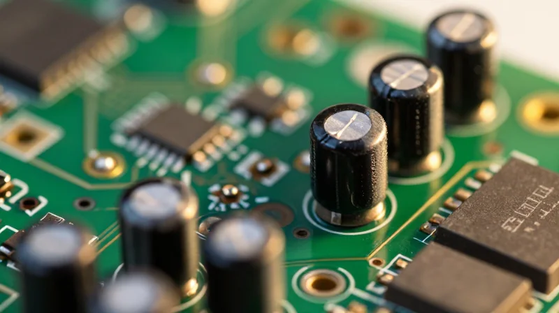
The fundamental rule for low-power ESL design is the minimization of loop inductance between decoupling capacitors and the load. To ensure the five-year battery performance metric, every decoupling capacitor must be placed as close as possible to the power pin of the IC it supports. This proximity prevents high-frequency noise from inducing parasitic voltage drops that force the power management system into inefficient operating states.
| Component Type | Placement Priority | Key DFM Constraint |
|---|---|---|
| Bulk Decoupling | Near Power Entry | Maintain Low ESR Path |
| High-Freq Bypass | Directly at IC Pin | Minimize Via Inductance |
| Oscillator Caps | Adjacent to XTAL | Isolate from Noise |
Oscillator Layout and Noise Isolation
Oscillators represent critical nodes where timing jitter can lead to unnecessary MCU wake-up cycles and increased current consumption. By maintaining a 'Keep-Out' zone around the crystal and its load capacitors, you effectively eliminate EMI interference from digital switching lines that would otherwise degrade clock stability and battery longevity.
Frequently Asked Questions on Component Positioning
- How does via-in-pad technology affect power consumption?
Via-in-pad reduces trace length and parasitic inductance significantly, lowering the energy wasted during high-frequency switching and protecting the battery budget. - Should oscillators be shielded with ground pours?
Yes, surrounding the oscillator circuit with a dedicated ground pour helps suppress crosstalk, preventing the MCU from misinterpreting clock signals and triggering false interrupt loops.
Advanced Trace Routing to Curb Parasitics
Mitigating Parasitic Capacitance via Routing Geometry
To achieve five-year battery performance in ESL systems, designers must treat every trace as a potential capacitor. Parasitic capacitance, specifically interlayer coupling, directly degrades the efficiency of power delivery networks (PDN) and consumes precious nano-amperes through leakage. By optimizing trace geometry—specifically width and inter-trace spacing—designers can drastically reduce dielectric absorption and maintain the strict voltage stability required for ultra-low-power microcontrollers.
Comparative Analysis: Standard vs. Parasitic-Aware Routing
| Parameter | Standard DFM Rule | Low-Power ESL Optimization |
|---|---|---|
| Trace Width | Constant for impedance | Minimized to reduce overlap area |
| Inter-trace Spacing | Minimum manufacturing gap | 3x-5x dielectric height to reduce coupling |
| Ground Plane | Solid pour | Segmented islands for analog/digital isolation |
Strategic Ground Plane Segmentation
A common pitfall in high-density low-power PCBs is the misuse of a monolithic ground plane. While ideal for RF, a unified plane can create 'return path noise' that triggers false state changes in high-impedance logic nodes. Implement ground segmentation to partition high-speed digital switching loops away from sensitive analog sensor inputs, ensuring that current returns do not overlap near high-gain amplifier stages.
FAQ: Advanced Routing for ESL Devices
- How does trace length affect battery drain?
Increased trace length adds series resistance and total surface area for capacitive coupling, leading to higher power consumption through ohmic losses and parasitic charging currents. - Should I use thinner traces for all signals?
No; while thinner traces reduce capacitance, they increase DC resistance. Balance width to keep IR drop below 1% of the supply voltage while minimizing parallel-plate capacitance. - Is via-stitching necessary for low-power?
Via-stitching is critical to minimize the loop area of return paths. A well-stitched reference plane ensures that the return current path is strictly controlled, preventing the spread of EMI that would otherwise shorten battery life.
Mitigating Leakage Currents in Passive Components

Selecting Components for Ultra-Low Leakage
To achieve a five-year lifespan, components must be selected not only for their functional performance but for their parasitic characteristics during sleep states. Leakage current is primarily driven by internal dielectric conduction and suboptimal encapsulation materials. Engineers should prioritize components with high insulation resistance (IR) ratings, particularly for decoupling capacitors and sensitive signal passives, to ensure standby currents remain in the nano-ampere range.
| Component Type | Preferred Material/Dielectric | Leakage Risk |
|---|---|---|
| Capacitors | C0G/NP0 Ceramic | Minimal (High IR) |
| Resistors | Thin Film Metal | Low (Stability focus) |
| Switches | Hermetically Sealed | Low (Isolation focus) |
Mitigating Surface Current Leakage
Surface contamination and humidity-induced leakage represent the greatest threats to deep-sleep power budgets. Even trace amounts of ionic flux residue or moisture can create conductive paths between closely spaced pins on high-impedance nodes. Implementing a stringent cleaning process and employing hydrophobic conformal coatings are essential DFM steps to maintain high surface resistance.
Best Practices for DFM Layout
- How does PCB cleanliness impact leakage?
Ionic residues from manufacturing flux act as electrolytes when moisture is present, drastically reducing surface resistance and enabling leakage paths between VCC and GND or signal pins. - Why avoid standard X7R capacitors in sleep-sensitive circuits?
X7R materials often exhibit higher dielectric absorption and self-discharge compared to C0G/NP0 variants, making them less suitable for battery-critical decoupling. - What is the role of guard rings?
Guard rings tied to a stable reference potential act as a shield around sensitive input nodes, diverting surface leakage current away from the high-impedance terminal.
DFM Rules for Mass Production Reliability
DFM Rules for Mass Production Reliability
Achieving a five-year battery lifecycle requires more than just efficient firmware; it demands a manufacturing process that minimizes variance in parasitic effects and material degradation. To ensure consistent power performance across thousands of units, designs must prioritize solder joint integrity, PCB cleanliness, and substrate stability.
Critical Manufacturing Constraints
| Design Rule | Impact on Longevity | Recommended Practice |
|---|---|---|
| Solder Mask Clearance | Prevents shorting/leakage | Minimum 50um web clearance |
| Via Plugging/Filling | Reduces trapped flux | Use epoxy-filled conductive vias |
| Surface Finish | Prevents oxidation/corrosion | ENIG or ENEPIG for low-leakage |
For devices operating at microamp current budgets, even trace levels of ionic contamination or oxidation can bridge high-impedance nodes, leading to battery drain. Implementing strict cleaning validation cycles post-assembly is mandatory.
Common Manufacturing Reliability Queries
- How does PCB surface finish influence low-power battery life?
Improper surface finishes can create porous interfaces prone to humidity absorption, increasing surface leakage currents. ENEPIG is preferred for its superior corrosion resistance and consistent contact impedance. - Why is via-in-pad technology risky for ESL devices?
If not perfectly capped, flux residue can hide within the via barrel. Over five years, this residue can become conductive under high-humidity conditions, causing localized power drain. - What testing protocol ensures consistent power rails in mass production?
In-circuit testing (ICT) should be augmented with flying probe testing that specifically checks for insulation resistance across high-impedance sleep-mode circuits.
Verification and Validation Testing
Bridging Design Intent with Measured Reality
Verification is the systematic process of checking if the PCB design adheres to low-power DFM rules, while validation ensures that the assembled prototype meets the strict energy budget required for multi-year operation. In ultra-low-power Electronic System Level (ESL) design, the goal is to identify 'ghost' power consumption—unseen leakage current—before moving to mass production.
Methodologies for Parasitic Drain Detection
| Testing Method | Objective | Detection Capability |
|---|---|---|
| Dynamic Power Profiling | Analyze current across sleep-to-active cycles | High-frequency spikes |
| Thermal Imaging | Locate hotspots indicative of leakage | Micro-short circuits |
| Static Leakage Mapping | Measure nano-ampere floor current | Passive component seepage |
To achieve five-year performance, engineers must utilize source measure units (SMUs) capable of sub-microampere resolution. Prototyping must focus on pruning parasitic paths introduced by board contaminants, high-impedance trace coupling, and non-optimized pull-up resistor networks.
FAQ: Validating Battery Performance
- How do I isolate leakage currents during validation?
Utilize a segmented power rail approach where individual domains are gated. Measure current on each segment to isolate leakage to specific sections of the PCB layout. - Why does my prototype fail at temperature extremes?
Material properties change with temperature. Validation must include environmental stress screening to ensure leakage paths don't open up when dielectric constants shift. - What constitutes a 'clean' power profile?
A clean profile displays a consistent, flat floor current during deep-sleep states with minimal transient oscillation, ensuring no unintended peripheral activation.
Achieving multi-year battery life in ESL devices is not an accident—it is the direct result of disciplined DFM adherence and rigorous design optimization. By mitigating parasitic capacitance and leakage paths early in the development lifecycle, you can ensure your product exceeds market longevity expectations. Ready to optimize your hardware stack for extreme efficiency? Contact our engineering team today for a comprehensive design review.
