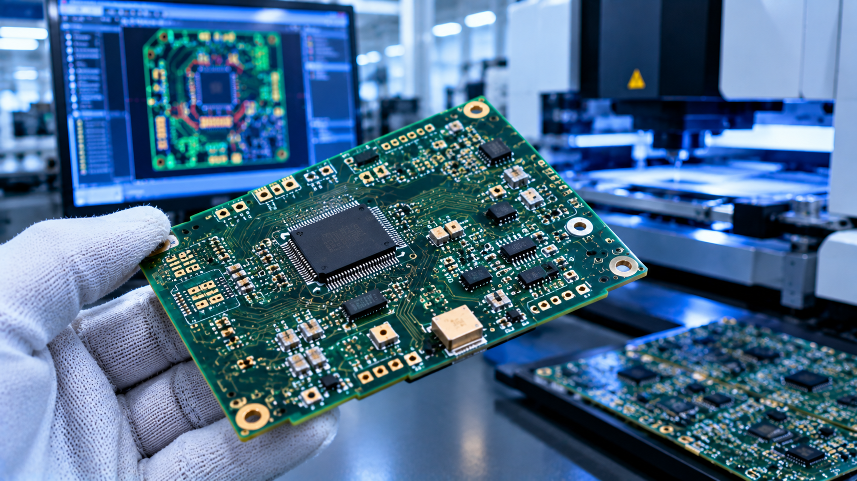
Introduction: Understanding PCB terminology is essential for hardware engineers, procurement teams, and anyone communicating with manufacturers. This guide explains PCB construction—substrate, copper foil, solder mask, silkscreen—and defines the key terms used in PCB design, fabrication, and assembly.
Description: Based on AnyPCBA's small-to-medium volume PCB and PCBA manufacturing experience, this guide explains PCB construction and defines the essential terms used in PCB design, fabrication, and assembly.
This article explains the structure of a PCB and the common terminology used in the field—helping engineers and procurement teams communicate more accurately with manufacturers.
Before PCBs existed, circuits were built using point-to-point wiring. This method had low reliability: as circuits aged, broken wires caused open or short circuits at connection nodes.
Wire wrapping improved durability by wrapping small-diameter wire around connection posts. As the industry moved from vacuum tubes and relays to silicon semiconductors and integrated circuits, component size and cost dropped. Electronics increasingly entered consumer markets, pushing manufacturers toward smaller, more cost-effective solutions. The PCB was born.
A PCB looks like a layered cake—different material layers are pressed together using heat and adhesive.
The PCB substrate is generally fiberglass. In most cases, this refers to FR4 material, which gives the PCB its rigidity and thickness. There are also flexible circuit boards made on polyimide or similar materials.
Cheap PCBs and perfboards use epoxy or phenolic materials—less durable but much cheaper. Phenolic materials have a low thermal decomposition temperature; excessive soldering time causes carbonization and an unpleasant smell.
The copper foil layer is pressed onto the substrate using heat and adhesive. On double-sided boards, copper foil is pressed onto both sides. Different PCB designs may have as few as 1 copper layer, or more than 16 layers.
Copper thickness is measured by weight—the weight of copper covering one square foot (ounces, oz). Most PCBs use 1oz copper; high-power PCBs may use 2oz or 3oz. This equals roughly 35μm or 1.4mil.
Above the copper layer is the solder mask. It covers the traces, preventing contact with other metals, solder, or conductive objects that could cause short circuits. Solder mask also allows soldering in the correct places and prevents solder bridging.
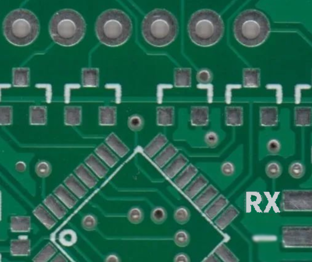
As shown in the image, solder mask covers most of the PCB but exposes silver annular rings and SMD pads for soldering. Generally green, but almost any color can be used.
Above the solder mask is the white silkscreen layer. Letters, numbers, and symbols are printed on it to facilitate assembly and help people understand the board design. The most common silkscreen color is white, but it can be made in almost any color. Multiple silkscreen colors on a single board are rare.
| Term | Definition |
|---|---|
| Annular Ring | The copper ring around a plated hole on a PCB |
| DRC | Design Rule Check—checks a design for errors such as shorted traces, traces too thin, or holes too small |
| Drill Hit | The deviation between the required and actual drill position. Incorrect drill centers from dull bits are a common manufacturing problem |
| Gold Finger | Exposed metal pads on the edge of a board, used to connect two circuit boards (expansion modules, memory sticks, older game cards) |
| Castellated Hole | Besides V-Cut, another depaneling design method. Continuous holes form a weak connection point for easy separation from the panel |
| Pad | An exposed portion of metal on the PCB surface, used for soldering components |
| Panelization | A large board composed of many separable small boards, speeding up automated production |
| Stencil | A thin metal or plastic template placed on the PCB during assembly, allowing solder paste through specific areas |
| Pick-and-Place | The machine or process that places components onto the circuit board |
| Plane | A continuous section of copper, defined by boundaries rather than a path. Also called a copper pour |
| Plated Through-Hole | A hole containing an annular ring and plated hole wall—a connection point, signal transition point, or mounting hole |
| FABFM | A through-hole resistor whose leads pass through PCB vias; the plated wall connects traces on both sides |
| Pogo Pin | A spring-supported temporary contact point, generally used for testing or programming |
| Reflow Soldering | Melting solder to connect SMD pads and component leads |
| Slot | Any non-circular hole. May be plated or non-plated; adds cutting time and cost. Edges cannot be perfectly right-angled because cutting tools are circular |
| Solder Paste Layer | A layer of solder paste formed on SMD pads via stencil before component placement. During reflow, it melts to form reliable electrical and mechanical connections |
| Solder Pot | A pot for soldering through-hole components, containing molten solder. The board passes rapidly over it to solder exposed leads |
| Solder Mask | A protective film covering copper to prevent short circuits, corrosion, and other issues |
| Solder Bridge | Two adjacent pins accidentally connected by a small drop of solder |
| Surface Mount | An assembly method where components are placed on the board without leads passing through vias |
| Thermal Relief | Short traces connecting a pad to a plane. Improper thermal design makes the pad difficult to heat, causing sticky soldering and longer reflow time |
| Trace | A generally continuous copper path on a circuit board |
| V-Score | An incomplete cut on a board, allowing it to be snapped along a straight line |
| Via | A hole on a board, generally used to transition a signal from one layer to another |
| Tenting | Covering a via with solder mask to prevent soldering. Connector or component pin vias are generally not tented |
| Wave Soldering | A method for soldering through-hole components. The board passes at constant speed through a molten solder wave, soldering leads and exposed pads together |
As a factory focused on small-to-medium volume PCB and PCBA manufacturing, AnyPCBA uses these terms daily. Our manufacturing capabilities cover 2–64 layers, including HDI, rigid-flex, and high-frequency hybrid. We hold ISO 13485 (medical) and IATF 16949 (automotive) certifications.
During DFM review, we focus on confirming:
DRC completeness: shorted traces, trace width, and drill dimensions within process windows
Panelization design: whether V-Cut or castellated hole methods suit the board shape and component layout
Thermal relief design: whether large copper plane pads have proper thermal isolation
Via processes: whether vias are tented, covered, or used for via-in-pad
Copper thickness requirements: whether 1oz, 2oz, or thicker copper matches current requirements
Our engineers help you confirm the process details behind these terms at the design stage, so your boards are not only drawable, but stable and reliable to produce.
If you're working on PCB design, or want to learn more about terminology and process details, contact us through our website.
What terminology confusion have you encountered in PCB design? Share your experience in the comments.