
In the fast-paced world of rugged action camera design, space is at a premium, but performance demands are soaring. As devices shrink in size, the pressure on your PCB interconnects to maintain high-speed signal integrity and withstand extreme mechanical stress becomes the primary hurdle. This guide provides the strategic framework engineers need to select the right Micro HDI solutions that balance miniaturization with high-performance reliability.
The Evolution of Micro HDI in Compact Imaging
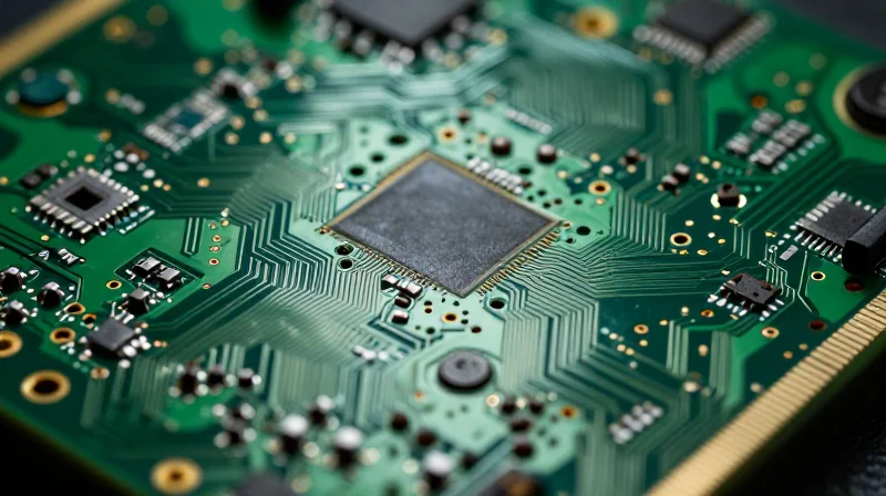
From Multilayer to Micro HDI: The Paradigm Shift
Traditional PCB design reached a physical ceiling with high-resolution image processing and smaller camera chassis requirements. The evolution to Micro HDI—characterized by laser-drilled microvias, sequential lamination, and fine-line geometry—allows engineers to pack denser processing power into smaller spaces. This is not merely about size reduction; it is about signal integrity. As action cameras push into 4K/60fps and 8K recording, the shortened trace paths inherent in Micro HDI designs drastically reduce electromagnetic interference (EMI) and signal loss, which are common failure points in legacy rigid-flex designs.
Impact of Interconnect Scaling on Rugged Imaging
| Feature | Legacy Multilayer | Micro HDI Technology |
|---|---|---|
| Via Structure | Mechanical Thru-Hole | Laser-Drilled Microvias |
| Trace/Space | 6 mil / 6 mil | 2 mil / 2 mil or less |
| Signal Integrity | Moderate (High Crosstalk) | Superior (Low Impedance) |
| Thermal Management | Basic | Advanced (Optimized Heat Paths) |
Frequently Asked Questions Regarding Micro HDI Selection
- Why is Micro HDI mandatory for action cameras?
Rugged action cameras require high-speed processors for image stabilization and encoding; Micro HDI supports the necessary component density and signal speed while maintaining a frame capable of surviving physical impact. - Does Micro HDI increase manufacturing complexity?
Yes. The adoption of sequential lamination and laser-drilled microvias requires high-precision fabrication, which must be accounted for during the design phase to avoid yield issues. - How does HDI design affect durability?
By reducing the total PCB surface area, we can build a more rigid, shock-resistant housing, decreasing internal component flex which is a primary cause of solder joint fatigue in high-impact scenarios.
Critical Signal Integrity Challenges in Miniaturized Layouts
Managing Electromagnetic Interference and Crosstalk
In the confined space of a high-performance action camera, components are placed in extremely close proximity, drastically increasing the risk of electromagnetic interference (EMI) and capacitive coupling. As traces shrink to meet high-density requirements, the electromagnetic field lines from one signal net can easily penetrate adjacent traces, leading to significant crosstalk. Designers must prioritize strict stack-up management, utilizing internal ground planes as references to confine magnetic flux and provide a low-impedance return path for high-speed digital signals.
The Challenge of Impedance Discontinuities
Maintaining a constant characteristic impedance is difficult in Micro HDI boards due to the frequent use of microvias and ultra-thin trace widths. Every transition, such as via stubs or changes in reference planes, creates a discontinuity that causes signal reflection and jitter. For high-speed sensor interfaces like MIPI CSI-2, even minor deviations in track geometry during the manufacturing process can compromise signal fidelity, leading to dropped frames or image artifacts in rugged conditions.
| Signal Integrity Issue | Common Cause | Mitigation Strategy |
|---|---|---|
| Crosstalk | Dense trace routing | Increase clearance, use differential pairs |
| Impedance Mismatch | Microvia transitions | Back-drilling, optimized landing patterns |
| EMI Emissions | Inadequate grounding | Solid reference planes, Faraday cage shielding |
Frequently Asked Questions
- How do microvias affect impedance?
Microvias introduce parasitic capacitance and inductance that can disrupt the transmission line impedance; these must be modeled accurately in 3D EM simulation tools. - Can I use standard FR-4 for Micro HDI?
While possible for low-speed signals, high-frequency imaging interfaces typically require low-loss, high-glass-transition temperature (Tg) materials to maintain signal integrity across thermal fluctuations common in action cameras.
Material Science: Selecting Substrates for Rugged Performance
The Role of CTE Matching in Thermal Resilience
In action cameras, the PCB is subjected to rapid thermal cycling, ranging from high-ambient heat during operation to sub-zero temperatures in extreme sports environments. A critical failure point is the mismatch between the Coefficient of Thermal Expansion (CTE) of the copper traces and the dielectric substrate. If the CTE values diverge significantly, the mechanical stress leads to barrel cracking in microvias and trace delamination. Engineers must prioritize materials with a low Z-axis CTE to prevent interconnect fatigue during repeated thermal expansion cycles.
Evaluating Low-Loss Laminates for Signal Clarity
High-performance action cameras require rapid data throughput for 4K and 8K video capture. Standard FR-4 materials often exhibit excessive dielectric loss (dissipation factor) at high frequencies, which attenuates high-speed signals. To maintain signal integrity, designers should specify high-frequency, low-loss laminates characterized by a stable Dielectric Constant (Dk) and low Loss Tangent (Df).
| Material Property | Rugged Requirement | Impact of Failure |
|---|---|---|
| Z-Axis CTE | Low (< 3.0%) | Microvia cracking and fatigue |
| Glass Transition (Tg) | High (> 170°C) | Delamination under thermal shock |
| Dissipation Factor (Df) | Ultra-low (< 0.005) | Signal degradation in high-speed links |
Frequently Asked Questions
- Why is Tg (Glass Transition Temperature) critical for rugged cameras?
A high Tg ensures the board remains rigid and stable at the elevated operating temperatures often generated by advanced image processors and sensors, preventing softening that could compromise connection reliability. - Is standard FR-4 ever suitable for modern micro HDI cameras?
Generally, no. Standard FR-4 suffers from inconsistent dielectric properties and poor thermal stability, which fail to support the dense, high-speed signals required by modern CMOS sensors. - How do I balance cost with high-frequency performance?
Opt for hybrid builds that use high-performance laminates only for critical signal layers and more cost-effective standard materials for ground planes and power distribution layers.
Advanced Thermal Management Strategies
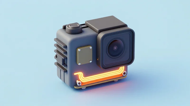
Advanced Thermal Management Strategies
In the confined, air-tight housings of rugged action cameras, traditional passive cooling is insufficient. The high heat density generated by processors and image sensors necessitates a holistic approach that treats the PCB as a structural heat spreader. Strategic placement of micro-vias, thermal land patterns, and copper-filled conductive paths are critical to routing heat away from sensitive components to the outer chassis.
Optimizing Via Structures for Thermal Relief
In HDI designs, micro-vias serve a dual purpose: interconnecting signal layers and providing a low-resistance path for thermal energy. Implementing 'thermal via stitching' beneath high-power components facilitates a direct vertical route for heat. For optimal results, utilize copper-filled blind and buried vias that provide a continuous metallic conduit to internal ground planes, effectively turning the PCB into an efficient heat radiator.
| Technique | Mechanism | Primary Benefit |
|---|---|---|
| Copper-filled Micro-vias | Vertical conductive channels | Reduces thermal resistance to inner planes |
| Thermal Land Patterns | Extended surface area pads | Improves junction-to-board heat transfer |
| Heat Spreading Copper Pour | High-density copper coverage | Distributes heat evenly across the PCB substrate |
Thermal Design FAQ
- How do blind and buried vias impact thermal performance?
Unlike through-hole vias, blind and buried vias minimize the footprint and electrical interference while providing dedicated vertical paths to inner-layer ground planes, allowing for concentrated heat sink integration. - Why is CTE (Coefficient of Thermal Expansion) alignment critical?
Action cameras undergo rapid temperature fluctuations; mismatched CTE values between the PCB substrate and the metallic thermal vias can cause structural fatigue and delamination over time. - Can I use external heat sinks with a compact HDI board?
Yes, by utilizing thermally conductive pre-preg and thermal interface materials (TIMs), the heat gathered by the internal copper layers can be coupled directly to the camera’s aluminum or magnesium external shell.
Designing for Mechanical Stress and Vibration
Mitigating Mechanical Stress in Micro HDI Assemblies
Action cameras are subjected to unpredictable kinetic energy, ranging from high-frequency motor vibrations to sudden impacts. In a Micro HDI PCB, the primary failure modes include solder joint fracture, via barrel cracking, and laminate delamination. To ensure structural integrity, designers must prioritize dynamic mechanical stability alongside electrical performance. This involves strategic component placement, enhanced board stiffening, and the utilization of high-Tg materials that resist mechanical fatigue under rapid thermal cycling.
Best Practices for Vibration-Resistant Layouts
- Component Anchorage
Use underfill or staking compounds for BGA packages and large ICs to distribute mechanical stress away from individual solder joints during high-G events. - Via Reliability
Utilize stacked and staggered microvia configurations with copper-filled processes to improve barrel structural integrity, preventing fracturing during board flexure. - Mounting Hole Isolation
Implement mechanical isolation through slotted mounting patterns or flexible mounting hardware to dampen high-frequency vibrations before they reach the PCB surface.
| Failure Mechanism | Design Mitigation Strategy | Impact on Durability |
|---|---|---|
| Solder Joint Fatigue | Solder mask defined pads + Underfill | High |
| Via Barrel Cracking | Copper-filled microvias + CTE matching | Critical |
| Board Flexure | Increased PCB thickness + Rigid-flex transition | Medium |
Frequently Asked Questions
- Does higher board thickness always equal better vibration resistance?
Not necessarily; while thicker boards are stiffer, they may transmit more energy to components. The optimal approach is to balance board stiffness with mechanical dampening through casing mounts. - Why is CTE matching crucial for rugged Micro HDI designs?
Action cameras operate in extreme temperature ranges; if the PCB laminate and components have mismatched CTEs, thermal cycling will induce constant mechanical strain on micro-interconnects, leading to eventual failure.
Manufacturing Standards and Reliability Protocols
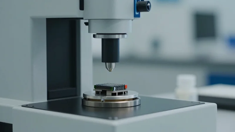
For high-performance action cameras, standard commercial PCB fabrication is insufficient. Engineers must mandate strict compliance with IPC Class 3 standards, which dictate the necessary reliability requirements for high-performance electronics. Achieving consistent performance under high-g shock and rapid thermal fluctuation requires a design-for-manufacturing (DFM) approach that prioritizes structural integrity alongside electrical performance.
Key IPC Standards for Rugged HDI Designs
| IPC Standard | Focus Area | Impact on Reliability |
|---|---|---|
| IPC-6012 Class 3 | Rigid PCB Performance | Ensures structural integrity of plating and internal interconnects. |
| IPC-2226 | HDI Design Standard | Defines requirements for microvias and thin dielectric structures. |
| IPC-4101 | Base Materials | Standardizes properties of prepregs and laminates for thermal stability. |
Essential Reliability Protocols
Reliability testing must simulate the lifecycle of an action camera, incorporating accelerated aging to identify failure points before mass production. Protocols should focus on the failure modes most common in small-form-factor HDI designs, specifically microvia fatigue and solder joint cracking.
- Thermal Shock Testing
Subjecting populated boards to rapid temperature transitions (e.g., -40°C to +85°C) validates the CTE matching between substrates and copper traces. - Highly Accelerated Life Testing (HALT)
Utilizing combined vibration and thermal stress to identify weak links in microvia structures and component solder connections. - Micro-section Analysis
Destructive physical analysis of test coupons to inspect copper wrap plating thickness and drill registration accuracy in buried vias.
Best Practices for Microvia Reliability
Microvias are the most frequent point of failure in HDI designs. To mitigate risk, designers should specify stacked or staggered microvia configurations that prioritize copper filling (electrolytic copper plating) to minimize internal voids. Avoiding 'via-in-pad' without proper capping can lead to solder wicking and compromised joints during the reflow process, which remains a primary concern in dense camera PCB assemblies.
The Role of Surface Finish in High-Frequency Design
Surface Finish Impacts on High-Frequency Signal Integrity
In high-frequency designs, the surface finish is not merely a corrosion protectant; it is an integral part of the transmission line geometry. The conductivity, roughness, and skin effect depth of the plating material significantly influence insertion loss and impedance control. For action cameras processing high-speed video data, choosing a finish that minimizes skin effect losses is vital to maintaining signal fidelity across compact, high-density traces.
Comparison of Common Finishes for Rugged HDI PCBs
| Finish | High-Frequency Performance | Solder Joint Reliability | Best Use Case |
|---|---|---|---|
| ENIG | Excellent | Moderate | Fine-pitch BGA/CSP components |
| ENEPIG | Very Good | High | Multi-cycle assembly & reliability |
| Immersion Silver | Superior | Moderate | Sensitive RF circuits |
Addressing Mechanical and Thermal Challenges
Action cameras undergo significant thermal cycling and vibrational shock. ENIG, while providing a flat surface for ultra-fine-pitch components, can be susceptible to 'black pad' syndrome if the immersion gold/nickel process is not tightly controlled. For maximum reliability, ENEPIG (Electroless Nickel Electroless Palladium Immersion Gold) is often preferred in ruggedized designs. The addition of a palladium layer acts as a barrier, preventing corrosion and ensuring superior solder joint strength under intense mechanical strain.
Frequently Asked Questions
- Why is ENIG preferred for high-density interconnects?
ENIG provides an extremely flat surface, which is essential for mounting high-pin-count BGA components typical in Micro HDI action camera designs. - Does ENEPIG affect high-frequency signal propagation?
While ENEPIG adds a layer of palladium, the thickness is strictly controlled to ensure that signal loss remains within acceptable parameters for modern high-speed interfaces. - How does surface roughness impact signal integrity?
Increased surface roughness due to finish deposition can increase resistive losses due to the skin effect, potentially degrading signal performance at multi-gigahertz frequencies.
Future-Proofing Your PCB Specification
Anticipating Next-Generation Throughput
As action camera sensors shift toward 8K resolution and higher frame rates, the micro HDI PCB must support exponentially faster data interfaces, such as MIPI C-PHY or newer SerDes standards. Future-proofing begins with over-specifying trace geometry to minimize impedance discontinuities and ensuring the stackup supports lower-loss materials that mitigate dielectric absorption at higher frequencies.
Design Strategies for Adaptability
| Design Factor | Legacy Approach | Future-Proof Strategy |
|---|---|---|
| Material Selection | Standard FR-4 | High-Tg, Low-loss Laminates |
| Via Topology | Thru-hole focus | Any-Layer HDI (ELIC) |
| Signal Routing | Loose constraints | Phase-matched differential pairs |
Frequently Asked Questions
- How does ELIC technology aid future-proofing?
Every Layer Interconnect (ELIC) allows for complete freedom in routing, which is essential when next-gen components require tighter pitch or more complex pin-out patterns. - Should I plan for modularity in my PCB?
Yes, incorporating modular daughterboard interfaces for sensor arrays allows you to upgrade imaging capabilities without redesigning the core processor board. - Is thermal management a concern for future hardware?
As data throughput rises, power consumption increases. Design dedicated internal ground planes to function as thermal spreaders to prevent hot spots in dense HDI clusters.
Selecting the optimal interconnect solution is the defining factor between a market-leading action camera and a field failure. By prioritizing signal integrity, thermal efficiency, and mechanical robust design, you ensure your device excels in any environment. Contact our engineering team today to review your current PCB specifications and accelerate your time-to-market with precision-engineered interconnect solutions.
