
Designing for the pet-worn electronics market requires a masterclass in efficiency. As manufacturers push for smaller, lighter, and more durable trackers, the PCB architecture becomes the heart of your project's success. Balancing complex GPS signal requirements with the physical constraints of an animal's collar is a challenge that requires precision engineering and strategic component selection.
The Triple Constraint: Weight, Waterproofing, and Signal Integrity
Designing a pet tracker requires reconciling three mutually restrictive design parameters: the physical necessity for low mass, the requirement for environmental hermetic sealing, and the need for high-frequency RF transparency. Every gram added to improve waterproofing or signal strength directly impacts the wearer's comfort and device longevity.
Managing the Interdependency of Design Constraints
| Constraint | Primary Conflict | Engineering Mitigation |
|---|---|---|
| Weight | Thick housings increase mass | Advanced polymers and PCB thinning |
| Waterproofing | Seals block antenna reception | RF-transparent hydrophobic coatings |
| Signal Integrity | Metals attenuate GPS signals | Optimized PCB layout and LNA placement |
Key Engineering Trade-offs
- How does waterproofing impact signal reception?
Traditional gaskets and thick overmolding can introduce dielectric constant shifts that de-tune the antenna, necessitating precise impedance matching adjustments during the board design phase. - Can I use metallic casings for durability?
Metallic enclosures act as Faraday cages, severely degrading GPS lock times. Utilize high-impact glass-filled nylon or RF-transparent PC-ABS instead to maintain signal integrity without sacrificing structural strength. - What is the best way to reduce weight without compromising strength?
Focus on high-density interconnect (HDI) PCB technologies that allow for smaller board surface areas, paired with localized potting rather than full-encapsulation, which saves significant weight.
To achieve a successful design, engineers must prioritize the antenna placement at the highest possible point relative to the animal's body to minimize multipath interference. By treating the GPS PCB as an integrated system—rather than a collection of components—you can successfully navigate the competing demands of miniaturization and reliability.
Optimizing Antenna Placement for GPS Reliability
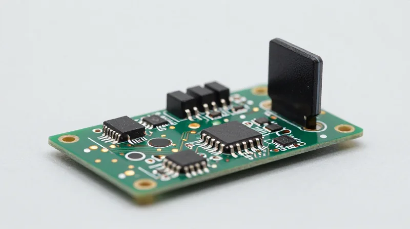
For pet tracking applications, antenna placement is the primary determinant of fix speed and accuracy. In a lightweight, waterproof PCB design, the antenna must be isolated from the high-frequency switching noise of power management systems and the signal-damping effects of the battery, all while maintaining a low-profile form factor that can withstand environmental exposure.
Minimizing Interference and Signal Obstruction
To achieve a stable satellite lock, prioritize the 'Clear View of the Sky' principle. Even in waterproof housings, signal attenuation is a critical risk factor. Follow these design strategies to maintain signal integrity.
- Component Isolation
Keep the GPS module and antenna at least 15mm away from the switching power supply and radio transmitters (like LTE-M or Bluetooth) to prevent EMI desensitization. - Ground Plane Strategy
Use an adequate ground plane to support the antenna's radiation pattern, but ensure it does not overlap with the battery or high-current traces, which can cause significant signal degradation. - Materials Compatibility
Select enclosure materials with low dielectric constants. Avoid carbon-fiber reinforced plastics or metallic paints, as they act as a Faraday cage, blocking GNSS signals.
Antenna Type Comparison
| Antenna Type | Performance | Profile | Best Use Case |
|---|---|---|---|
| Ceramic Patch | High | Medium | Large pet collars |
| Chip Antenna | Medium | Very Low | Micro-trackers |
| Active Patch | Very High | High | Deep forest tracking |
Prototyping Tips for Signal Testing
/* Implementation check for GPS Signal-to-Noise Ratio (SNR) */
if (gps.satellites.value() > 4 && gps.hdop.value() < 2.0) {
  transmit_location();
} else {
  log_interference_event();
}
Battery Management Systems (BMS) in Miniaturized Form Factors
BMS Integration in Miniaturized Form Factors
In pet tracker development, the BMS acts as the heartbeat of the device, managing energy flow from tiny lithium-polymer cells while protecting against over-voltage and thermal runaway. When miniaturization is a priority, standard off-the-shelf management circuits often occupy too much PCB real estate. Engineers must look toward highly integrated Power Management Integrated Circuits (PMICs) that combine voltage regulation, charging logic, and battery protection in a single, ultra-small package, often utilizing Wafer Level Chip Scale Packaging (WLCSP) to minimize footprints to just a few square millimeters.
Key Considerations for BMS Selection
| Feature | Constraint in Pet Trackers | Design Recommendation |
|---|---|---|
| Quiescent Current | Battery drain during idle | Select ICs with <5µA standby |
| Form Factor | PCB real estate limits | Prioritize WLCSP packaging |
| Charging Rate | Heat generation/Safety | Adjustable thermal regulation |
Frequently Asked Questions on BMS Design
- How does the BMS impact waterproof integrity?
A poorly designed BMS may require multiple external components and vias, complicating the PCB layout and potentially creating entry points for moisture. Integrated PMICs reduce component count, allowing for cleaner board layout and easier conformal coating. - Can I use a standard mobile phone BMS for my pet tracker?
Usually no; mobile BMS chips are designed for larger cells. Pet trackers require high-precision fuel gauging for micro-batteries (e.g., 100mAh to 300mAh) to ensure accurate reporting of the remaining life to the pet owner. - What is the primary trade-off between BMS size and battery life?
Highly integrated tiny BMS chips sometimes lack advanced power-path management features. You must balance the need for an ultra-small PCB against the necessity of efficient dynamic power routing to maintain long GPS acquisition intervals.
PCB Material Selection for Ruggedized Wearables
Evaluating Substrate Materials for Harsh Environments
For pet-wearable GPS devices, the PCB material must withstand high mechanical stress and constant exposure to environmental contaminants while maintaining an ultra-lightweight profile. Standard FR-4, while cost-effective, often fails to provide the long-term humidity resistance required for outdoor animal activity. Designers should prioritize high-glass-transition-temperature (Tg) materials or advanced polyimide substrates to ensure consistent signal integrity under varying thermal and moisture conditions.
| Material Type | Weight Impact | Moisture Resistance | Best Application |
|---|---|---|---|
| High-Tg FR-4 | Medium | Moderate | Standard outdoor trackers |
| Polyimide (Flexible) | Ultra-Low | High | Curved/Ultra-compact housings |
| Ceramic-Filled PTFE | High | Excellent | High-frequency GPS antennas |
| Halogen-Free Laminates | Low | Good | Eco-conscious rugged designs |
Key Considerations for Substrate Selection
- How does moisture absorption affect signal precision?
Materials like standard FR-4 absorb moisture, which changes the dielectric constant (Dk) and dissipation factor (Df). This leads to impedance mismatches that degrade GPS signal reception. - Why is the Glass Transition Temperature (Tg) important?
A higher Tg ensures the PCB remains dimensionally stable when the pet is exposed to direct sunlight or high-activity heat, preventing micro-cracking in solder joints. - Should I use Rigid-Flex designs for weight reduction?
Rigid-flex allows for a smaller housing by eliminating heavy connectors and bulkier cabling, effectively reducing the overall weight while maintaining high structural robustness.
When finalizing the material stack-up, it is vital to balance substrate thickness with the overall device enclosure constraints. Choosing thinner copper foils and micro-via technologies allows for higher routing density without the need for additional layers, keeping the PCB weight well within the limits required for small pet comfort.
Enclosure-Compatible Layout Techniques
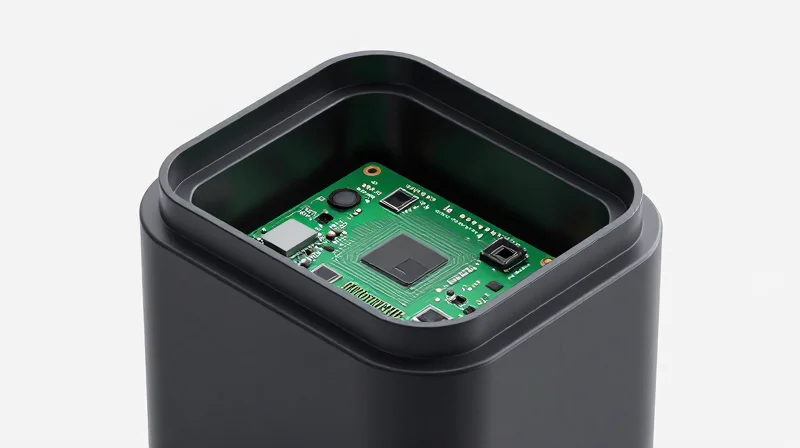
For IP67 and IP68-rated enclosures, the PCB must not only function electronically but serve as a structural element that accommodates seals and prevents interior volume waste. Designing for these rugged environments requires balancing component density with the necessity of maintaining a low-profile board that avoids interference with gaskets or cable glands.
Contouring and Mechanical Constraints
The PCB outline should mirror the inner geometry of the enclosure shell. By using 3D CAD integration, designers can define "keep-out" zones around screw bosses, o-ring grooves, and ultrasonic welding beads. Maintaining a clearance of at least 0.5mm between the board edge and the internal wall of the enclosure is recommended to account for thermal expansion and assembly tolerances.
Component Density Optimization Strategies
| Component Type | Placement Strategy | Benefit |
|---|---|---|
| GPS/Cellular Module | Top-side, edge-adjacent | Improved signal path clearance |
| Passives (0201/01005) | Bottom-side | Reduced PCB footprint area |
| High-Mass Components | Fixed with potting/epoxy | Mechanical stability during impact |
Best Practices FAQ
- How does PCB thickness impact waterproof integrity?
A 0.8mm or 1.0mm board is often preferred for lightweight designs; however, it must be rigid enough to prevent flexing, which could compromise the seal integrity of the enclosure gaskets during movement. - Why should I use blind or buried vias?
These techniques allow for higher trace density without increasing board layer count, saving critical vertical space and reducing the overall volume required inside the waterproof casing. - How should connectors be handled for IP68 ratings?
Minimize external connectors where possible by using wireless charging and Bluetooth/NFC for diagnostics; if physical connectors are mandatory, use bulkhead-sealed versions flush-mounted to the casing wall.
Mitigating EMI and Signal Noise in Compact Designs

Minimizing Signal Noise in High-Density Layouts
In lightweight GPS pet trackers, the proximity of high-frequency components—such as cellular modules, GNSS receivers, and switching power supplies—often leads to electromagnetic interference (EMI). To maintain data integrity, developers must utilize a multi-layer stack-up that prioritizes signal return paths and physical isolation.
- Why is a solid ground plane essential?
A continuous ground plane beneath signal layers provides the shortest return path for high-frequency currents, significantly reducing loop area and minimizing inductive EMI radiation. - How can differential pair routing help?
By routing sensitive lines like USB or high-speed data as differential pairs, you ensure that noise coupled into the lines is common-mode, allowing for cancellation at the receiver and improving signal-to-noise ratios.
Shielding Strategies for Restricted Enclosures
When space constraints prevent large physical separations, board-level shielding (BLS) becomes mandatory. Using lightweight, low-profile metallic cans directly soldered to the PCB covers sensitive RF circuits, creating a Faraday cage that isolates noise sources from susceptible traces.
| Mitigation Strategy | Best Application | Impact on Weight |
|---|---|---|
| Board-Level Shields (BLS) | RF/Cellular Modules | Low |
| Via Stitching | Edge Radiations | Negligible |
| Ferrite Beads | Power Supply Lines | Negligible |
PCB Layout Best Practices
# Critical Layout Guidelines
1. Keep GPS antenna traces as short as possible with controlled impedance (50 Ohm).
2. Isolate high-speed digital switching logic from sensitive analog RF front-ends.
3. Implement dedicated ground planes for analog and digital domains, connected at a single star point if necessary.
4. Ensure all vias connecting to ground planes are stitched to prevent edge resonance.
Thermal Management for Sealed Pet-Worn Devices
Managing heat in a completely sealed environment is a critical engineering hurdle for pet trackers. Since active ventilation is not an option for IP-rated enclosures, the device must function as its own heat sink. Thermal management for these compact units relies on transferring heat from power-intensive components like the GPS module and cellular radio directly to the device casing, ensuring that thermal accumulation does not degrade the battery or sensitive electronics.
Conductive Thermal Path Strategy
The most effective method for dissipating heat in a sealed, lightweight PCB involves creating a direct thermal bridge. By placing thermal vias beneath high-heat components, designers can move heat to the bottom side of the PCB, which is then coupled to the device housing using a thermally conductive gap pad or silicone interface material.
| Thermal Strategy | Effectiveness | Weight Impact |
|---|---|---|
| Thermal Vias to Chassis | High | Negligible |
| Copper Pour Heat Sinks | Moderate | Low |
| Internal Aluminum Heat Spreader | Very High | Moderate |
Thermal Management Best Practices FAQ
- How do I prevent heat buildup without vent holes?
Utilize the enclosure casing as a heat sink. By placing high-power components near the enclosure wall and using high-thermal-conductivity interface pads, heat is moved out of the PCB and dissipated through the shell surface. - What is the role of the copper pour?
A large copper pour acts as a thermal mass, absorbing heat peaks from short-burst GPS transmissions or cellular data uploads, effectively spreading the heat across a larger surface area to prevent hotspots. - Can I use thermal grease in a sealed unit?
Avoid standard thermal grease as it can leak or dry out over time. Instead, use cured thermally conductive adhesives or high-durability gap pads that provide a permanent, non-contaminating thermal bridge.
Prototyping Considerations
Always validate your thermal design with IR thermal imaging under real-world usage scenarios. Pet trackers often operate while moving through different ambient temperatures; ensure your PCB thermal management can handle the peak operating temperature of the cellular modem during high-power transmission cycles to prevent protective thermal throttling.
Prototyping and Testing for Real-World Pet Activity
Simulating the Pet-Worn Environment
To validate a pet tracker prototype, you must move beyond standard lab conditions. Real-world pet activity involves cyclical stress, moisture ingress, and high-frequency vibrations. Your testing protocol must replicate these physical demands using environmental chambers and mechanical stress fixtures, ensuring the PCB, interconnects, and waterproof seals maintain integrity over time.
Key Stress Testing Parameters
| Stress Factor | Test Method | Goal |
|---|---|---|
| Moisture/Liquid | Submersion (IPx7/8) | Verify enclosure seal and PCB conformal coating integrity. |
| Shock/Impact | Drop & Collision Simulation | Prevent solder joint fracturing in dense board layouts. |
| Vibration | Variable Frequency Sweep | Ensure high-frequency GPS antennas and crystals remain stable. |
Iterative Validation Cycles
Early-stage prototyping should utilize rapid 3D-printed housings that mimic the final mass and center of gravity of the device. By testing early, you can isolate mechanical failure points—such as PCB bending during rapid movement—before committing to expensive injection-molded production runs.
Frequently Asked Questions
- How do I test for waterproof integrity in the prototype phase?
Utilize vacuum decay testing or localized pressure immersion tests on early enclosure designs before integrating the full PCB assembly. - What is the most common cause of PCB failure in pet trackers?
Solder joint fatigue caused by continuous, high-frequency impacts during running or jumping is the primary failure mode in lightweight units. - Should I use conformal coating before or after testing?
Apply high-grade conformal coating during initial prototyping to ensure that your protection strategy does not interfere with signal performance or introduce thermal bottlenecks.
Choosing the right PCB architecture is the difference between a market-leading product and a prototype that fails in the field. By prioritizing signal health and structural efficiency from day one, your development team can ensure long-term durability and accurate performance. Ready to optimize your hardware design? Contact our engineering team today to discuss your specific project requirements.
