
In the race to shrink electronics, rigid-flex PCBs have become the backbone of modern innovation. However, the transition from rigid boards to flexible interconnects is a minefield for the unprepared. Failing to adhere to strict DFM protocols during the layout stage leads to cracked traces, delamination, and signal degradation. This guide distills twenty years of manufacturing expertise into the essential rules you need to optimize yield and ensure your circuits survive the stresses of the real world.
Understanding the Mechanics of Rigid-Flex Reliability
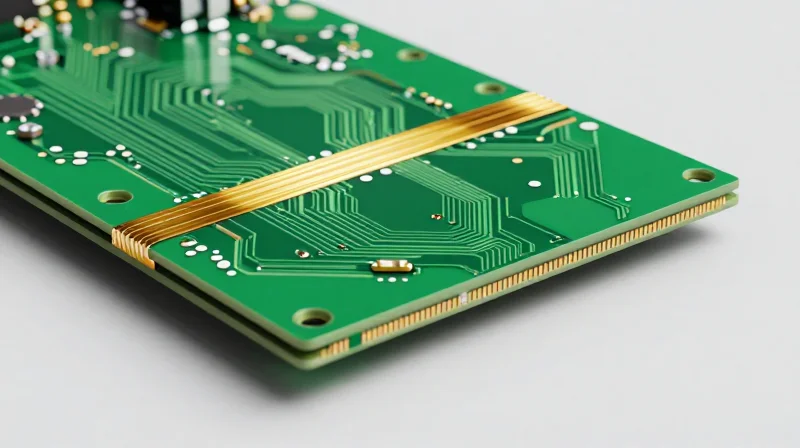
The Shift from Static to Dynamic Substrates
In standard rigid PCB design, reliability is largely determined by thermal expansion and signal integrity. However, in the context of TWS devices, the rigid-flex transition zone introduces complex mechanical loading. The fundamental DFM challenge lies in the fact that flexible polyimide circuits are not merely thinner PCBs; they are dynamic components that undergo repeated strain, bending, and torsion. Failing to account for the material's modulus of elasticity during the design phase often leads to copper fatigue at the rigid-to-flex interface, the most common failure point in compact electronics.
Material Behavior and Mechanical Constraints
| Parameter | Rigid FR-4 | Flexible Polyimide |
|---|---|---|
| Flexural Modulus | High (Rigid) | Low (Elastomeric) |
| CTE X/Y Axis | Low | High |
| Failure Mode | Delamination | Copper Work-Hardening |
Key Reliability FAQs
- Why do standard rigid via rules fail in flex regions?
Rigid designs rely on plated through-holes (PTH) that are structurally brittle. When placed within a flex area, the stress concentration causes the barrel-to-pad interface to crack almost immediately upon installation into a compact housing. - How does bending radius impact signal integrity?
A radius that is too tight induces micro-stretching of copper traces, altering their width and impedance. In high-frequency TWS antenna or audio signals, this causes unintended signal degradation. - What is the role of the transition zone?
The transition zone acts as a buffer. Proper DFM dictates a 'tapered' rigid-flex interface to distribute mechanical stress away from the junction point, preventing immediate fatigue.
Mastering Bend Radii and Flex-Zone Geometry

Calculating Minimum Bend Radii
The fundamental principle for preventing trace fracture in flex circuits is the 'Bend-to-Thickness' ratio. For high-precision TWS applications, where space is at a premium, copper traces must be positioned at the neutral axis to minimize tensile and compressive strain during bending cycles. As a rule of thumb, the internal bend radius (R) must be at least 10 to 20 times the total thickness of the flexible substrate (h) to avoid mechanical failure.
| Flex Construction Type | Recommended Bend Radius Factor | Failure Risk Level |
|---|---|---|
| Single-Sided Flex | 6x - 10x total thickness | Low |
| Double-Sided Flex | 12x - 20x total thickness | Moderate |
| Multi-Layer Flex | 20x - 40x total thickness | High |
Optimizing Flex-Zone Geometry
To prevent stress concentration at the transition between rigid and flexible areas, designers must implement a 'tapered' or 'filleted' copper approach. Abrupt changes in material stiffness create fatigue hotspots. Always use rounded fillets at the junction of rigid-flex interfaces and avoid placing vias within 1mm of the bend transition to ensure the long-term reliability of the TWS device.
Frequently Asked Questions on Flex Reliability
- Can I place components on the bend area?
No. Components and solder joints are rigid and prone to cracking under flexure. Keep all components at least 2mm away from any bend transition zone. - Does the orientation of copper traces matter?
Yes. Traces should be routed perpendicular to the bend line whenever possible and utilize curved, rather than sharp, angular patterns to distribute mechanical stress. - How does coverlay choice affect bend capability?
Polyimide coverlays are preferred over solder mask for flex areas; they provide better strain relief and higher mechanical durability during repeated bending cycles.
Copper Grain Direction: Why Orientation Matters
The Physics of Copper Grain and Fatigue Resistance
Copper foil, particularly the rolled-annealed (RA) variety used in flexible circuits, possesses a directional grain structure formed during the manufacturing process. When subjected to mechanical stress, copper exhibits anisotropic behavior; it is significantly more resistant to cracking when tensile or compressive forces are applied perpendicular to the grain orientation. Aligning traces parallel to the rolling direction creates a pathway for crack propagation along the grain boundaries, which drastically reduces the cycle life of the flex circuit.
Best Practices for Trace Layout
For ultra-compact TWS enclosures, where repetitive bending or tight static folds are inevitable, adhere to the following design constraints to maximize longevity:
- Perpendicular Routing
Always route signal traces perpendicular to the bend axis. This configuration ensures the grain structure resists the strain of the fold rather than facilitating fracture. - Avoid Sharp Angles
Use generous radii for all trace turns within the flex zone. Abrupt changes in direction create stress concentration points that are hypersensitive to grain orientation. - Avoid Via Placement
Strictly prohibit the placement of vias or through-holes within the active flex zone, as they create structural discontinuities that bypass the benefits of grain alignment.
| Orientation | Fatigue Life | Application Recommendation |
|---|---|---|
| Parallel to Bend Axis | Low | Avoid in active flex zones |
| Perpendicular to Bend Axis | High | Primary choice for reliable flex |
| Diagonal/Angled | Moderate | Use only when space is absolute constraint |
Communicating Requirements to PCB Fabricators
It is insufficient to merely layout the board correctly; you must communicate the copper grain orientation to your fabricator. Specify that the 'machine direction' of the copper foil must be aligned such that it is perpendicular to the bend axis of the flex zones. Failure to explicitly include this in your fabrication drawing (FAB notes) may result in the manufacturer orienting the board panels for maximum material yield rather than reliability, leading to latent field failures in your TWS product.
Optimizing Layer Transition Zones (The Rigid-Flex Interface)
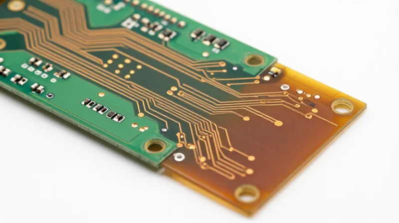
The Interface Paradox: Managing Material Mismatch
The transition zone—the boundary where a rigid FR4 board terminates and the polyimide flex circuit begins—is a significant mechanical discontinuity. Because the modulus of elasticity differs sharply between rigid and flexible substrates, cyclic stress in TWS devices during charging or case manipulation can lead to copper delamination or trace cracking at this interface. To minimize stress concentration, you must implement a gradual transition of material stiffness and avoid sudden geometric changes that act as stress risers.
Best Practices for Pad Anchoring and Relief
- Use Anchored Pads
Ensure every copper trace terminating at the rigid-flex interface features an anchoring spur or 'dog-bone' shape. This distributes peel forces across a larger surface area, preventing the copper from lifting during bending. - Staggered Trace Lengths
Avoid parallel termination points. Staggering the endpoints of traces creates a 'stepped' stiffness profile, which prevents a single line of stress from fracturing all signals simultaneously. - Coverlay Pullback
Ensure the coverlay terminates at least 0.5mm past the rigid-flex junction. This overlap provides a buffer that supports the copper traces as they transition from the rigid support to the unsupported flex region.
Transition Zone Design Comparison
| Feature | High-Risk Design (Avoid) | DFM Optimized (Recommended) |
|---|---|---|
| Trace Termination | Flush at transition line | Staggered by 0.2mm to 0.5mm |
| Pad Geometry | Square/Standard pads | Rounded, anchored spurs |
| Coverlay | Ends at rigid junction | Overlaps into rigid by 0.5mm |
| Copper Planes | Solid plane at transition | Hatched/Cross-hatched planes |
Finally, avoid placing surface-mount components near the rigid-flex interface. The thermal expansion coefficient of components like ceramic capacitors can induce stress into the board substrate, potentially cracking traces already under mechanical load due to the flex transition. Maintain a minimum keep-out zone of 1.5mm from the interface for all rigid-side components.
Signal Integrity in Dense, Multi-Layer Circuits

Managing Impedance in Flex Zones
In TWS-scale rigid-flex boards, maintaining a constant characteristic impedance across the transition from rigid FR-4 to polyimide flex is critical for high-speed signal integrity. The change in dielectric constant (Dk) and the lack of a continuous reference plane in the flex zone necessitate specialized stack-up design, such as using 'floating' ground planes or hatched copper patterns to maintain structural flexibility while providing sufficient return paths.
Stack-up Strategy Comparison
| Design Strategy | Signal Integrity Benefit | Mechanical Impact |
|---|---|---|
| Solid Reference Plane | Excellent shielding; high EMI control | High stiffness; risks delamination |
| Hatched Ground Plane | Moderate impedance control | High flexibility; reduced stress |
| Differential Pairs (No Ref) | Low impedance control | Maximum flexibility; high signal noise |
Minimizing Signal Reflections at Interconnects
Impedance discontinuities often occur at the rigid-to-flex interface due to PTH (plated-through-hole) geometry and the transition in dielectric materials. To minimize reflections, designers should implement impedance-matched transitions, keeping the return path as close to the signal trace as possible. Avoiding stubs and ensuring that the trace width is recalculated for the flex-specific Dk is non-negotiable for GHz-range TWS components.
Frequently Asked Questions
- How does hatched ground influence impedance?
Hatching increases the trace-to-plane distance, which typically raises impedance. You must increase trace width accordingly to compensate for the reduction in parasitic capacitance. - Should I use adhesive or adhesive-less flex?
Always prioritize adhesive-less polyimide laminates. The adhesive layers often have inconsistent dielectric properties that cause unpredictable impedance shifts in high-precision circuits. - How do I mitigate EMI in the flex segment?
Employ silver ink shielding or utilize outer-layer micro-coax structures if the board architecture allows, though balanced differential routing remains the most effective space-saving measure.
Selecting Materials for High-Yield Production
Material Selection Criteria for High-Flex Applications
In ultra-compact TWS devices, the choice of base materials dictates the survival rate of the interconnect. For high-precision rigid-flex boards, polyimide (PI) remains the industry standard due to its exceptional thermal stability, chemical resistance, and mechanical toughness. However, the specific resin system and adhesive formulation used to bond the flexible layers determine how the board manages internal stresses during tight-radius bending.
| Material Property | Requirement for TWS Boards | Impact on Performance |
|---|---|---|
| Dielectric Constant (Dk) | Low and Stable | Maintains high-speed signal integrity |
| Young's Modulus | Low | Increases flexibility and bend cycle life |
| Glass Transition (Tg) | High (>200C) | Prevents delamination during reflow |
| Moisture Absorption | <1.0% | Reduces risk of popcorning and electrical leakage |
Adhesiveless vs. Adhesive-Based Systems
For maximum durability, designers should prioritize adhesiveless copper-clad laminates (CCL). Adhesive-based systems introduce a distinct interface that acts as a stress concentration point, which is prone to fatigue cracking under repeated flexure. Adhesiveless laminates allow for a thinner construction profile and superior thermal dissipation, which is non-negotiable for the restricted airflow environment found in TWS housings.
FAQ: Material Engineering for Flex
- Why is coverlay material critical?
The coverlay provides essential insulation and mechanical protection. In high-density designs, using thin, low-modulus acrylic or epoxy-based coverlays is necessary to avoid stiffening the bend zone while providing sufficient barrier against moisture. - How does material thickness impact flex life?
The total thickness of the flexible section is the primary driver of strain during bending. Designers should minimize the copper weight and dielectric thickness to ensure the neutral axis of the circuit remains balanced. - Are there specific requirements for the bonding film?
In transition areas between rigid and flex zones, use B-stage bonding films with high elongation properties to buffer the mechanical mismatch and prevent micro-fractures at the interface.
Advanced DFM for Micro-Via and Pad Design
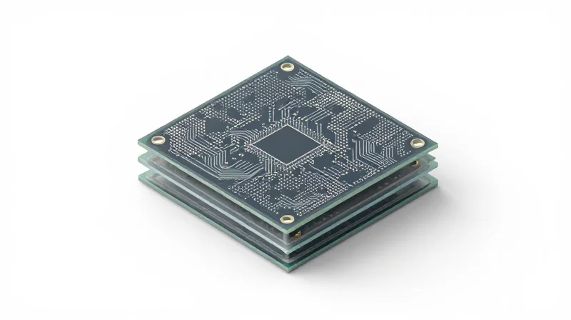
In the constrained form factor of TWS devices, micro-vias and pads serve as the structural weak points of the PCB assembly. Achieving high-yield production requires move away from standard rigid design rules toward specific geometric considerations that mitigate stress concentration and prevent delamination.
Advanced Pad Anchoring Strategies
Standard surface mount pads often fail at the rigid-flex interface due to poor adhesion under mechanical load. By incorporating 'anchoring spurs'—small traces of copper extending from the pad into the coverlay—designers can significantly increase the pull-strength of the pad, preventing lifting during bending.
| Feature | Design Rule | Reliability Benefit |
|---|---|---|
| Pad Filleting | Tear-drop pattern | Reduces stress concentrations at the trace-to-pad junction |
| Pad Anchoring | Copper spurs under coverlay | Prevents mechanical lifting during repeated flex cycles |
| Via Placement | Staggered/offset | Minimizes structural fatigue in the flex Z-axis |
Micro-Via Design for Flex Reliability
Micro-vias in flex sections must be designed to withstand tensile strain. Using stacked vias in thin flexible substrates is highly discouraged; instead, utilize staggered via configurations to distribute mechanical stress across a larger surface area.
- Why avoid laser-drilled blind vias near the bending radius?
These vias create localized stiffening and stress points that lead to micro-cracking in the copper barrel during dynamic flexing. - What is the ideal plating thickness for micro-vias in flex circuits?
Aim for a minimum of 20-25 micrometers of copper in the via barrel to handle the thermal expansion mismatch between the dielectric and the copper interconnect. - How does via-in-pad affect solder joint reliability?
Via-in-pad allows for higher density but requires non-conductive epoxy fill and over-plating to ensure a flat, stable surface that does not leach solder away from the component joint.
Prototyping Recommendations
/* Recommended Pad Filleting Rule */
# Define teardrop geometry
teardrop_min_width = trace_width * 1.5;
teardrop_length = pad_diameter * 0.4;
# Ensure no vias are within 1.0mm of the rigid-flex transition line
Verification and Simulation Techniques
Virtual Prototyping for Mechanical Resilience
In the context of TWS wearables, the rigid-flex interface is the most common point of failure. Engineers must utilize Finite Element Analysis (FEA) to simulate the stresses applied during device assembly and daily operation. By modeling the bend radius and material elasticity, designers can predict how the copper traces will respond to repetitive strain, allowing for geometry adjustments that mitigate stress concentration before committing to expensive physical prototypes.
Thermal Simulation and Signal Integrity
Ultra-compact form factors leave little room for heat dissipation, making thermal simulation vital. Coupled field analysis—where thermal expansion is integrated with signal integrity (SI) modeling—ensures that impedance deviations caused by temperature-induced material shifts do not exceed performance tolerances. High-speed signals are particularly sensitive to these fluctuations, requiring validation through 3D EM solvers.
| Verification Type | Focus Area | Simulation Goal |
|---|---|---|
| Mechanical FEA | Flex zones | Identify stress points in copper traces |
| Thermal Analysis | High-density zones | Verify temperature limits vs. material Tg |
| 3D EM Simulation | Interconnects | Ensure impedance stability across flex hinges |
Frequently Asked Questions
- How early should simulation start in the design cycle?
Simulation should begin at the layout stage, specifically during the stack-up definition, to ensure material properties are accurately reflected in the mechanical model. - Can standard EDA tools handle rigid-flex stress analysis?
While standard EDA handles electrical design, dedicated plug-ins or external FEA tools are required for accurate mechanical stress analysis and complex bending simulations. - Why is coupled field analysis important for TWS?
Coupled analysis accounts for the fact that heat expansion physically alters trace geometry, which directly impacts signal impedance—a critical factor for high-frequency wireless communication.
Successfully designing for rigid-flex is a balancing act between mechanical flexibility and electrical performance. By implementing these DFM rules, you mitigate risk, improve product longevity, and significantly reduce costly manufacturing iterations. Are you ready to optimize your next high-density project? Contact our engineering team today for a design review and ensure your board is production-ready.
