
Developing high-precision blood pressure monitors requires more than standard circuit design; it demands a synergy of rigorous signal integrity management and compact, DFM-focused engineering. For medical device manufacturers, the challenge lies in capturing minute pressure transducer signals without noise interference, all while fitting components into space-constrained enclosures. This guide walks you through the technical imperatives for achieving clinical-grade stability in your next PCBA project.
The Anatomy of a High-Precision Medical PCBA
The Anatomy of a High-Precision Medical PCBA
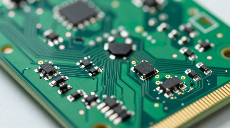
The architecture of a high-precision medical PCBA for blood pressure monitoring is defined by its ability to resolve micro-volt level pressure oscillations while maintaining immunity to electromagnetic interference (EMI). Unlike standard consumer electronics, these boards utilize a stratified design where analog front-end (AFE) components are physically isolated from digital switching noise to preserve signal integrity.
Critical Signal Path Components
The signal path is the most sensitive region of the PCBA. Achieving high-precision results requires a meticulous selection of components and routing strategies that minimize thermal drift and parasitic capacitance.
| Component Class | Role in Sensor Path | Design Constraint |
|---|---|---|
| Precision Op-Amps | Signal amplification | Ultra-low offset voltage drift |
| High-Resolution ADC | Data conversion | Low noise floor requirement |
| Reference Voltage IC | Signal stability | High thermal stability (low ppm/°C) |
Frequently Asked Questions
- Why is board layout crucial for blood pressure accuracy?
Small trace geometries and proximity to digital controllers can induce noise that masks the subtle oscillations produced by a pressure sensor. - How does thermal management affect precision?
Thermal gradients across the PCB can cause components like op-amps and resistors to drift, leading to inaccurate pressure readings during patient monitoring.
Optimizing Trace Routing for Low-Noise Analog Front-Ends

Minimizing Parasitic Noise and Crosstalk
In precision medical sensing, the analog front-end (AFE) is highly susceptible to EMI and crosstalk due to the low-voltage output of MEMS-based pressure transducers. Effective trace routing must prioritize short signal paths and consistent reference planes to suppress noise. Designers should minimize loop areas in the analog signal path to prevent the induction of unwanted currents that can distort blood pressure waveform acquisition.
| Design Strategy | Impact on Signal Integrity | Implementation Rule |
|---|---|---|
| Differential Pairs | Rejects Common-Mode Noise | Ensure equal length and tight coupling |
| Guard Traces | Reduces Crosstalk | Place ground vias at 5mm intervals |
| Reference Plane | Reduces EMI Emissions | Use a solid, contiguous ground plane |
Essential Routing Best Practices
- How does layer stack-up affect AFE performance?
Place analog signal layers between dedicated ground planes to provide an effective shield against high-frequency interference from digital or power sections. - What is the rule for trace separation?
Apply the '3W' rule—maintain a distance between parallel signal traces equal to three times the width of the trace—to significantly reduce inter-trace capacitive coupling. - How should I handle return paths?
High-speed digital traces must never route over split planes, as return currents will follow the path of least impedance, potentially creating massive EMI loops in sensitive analog regions.
Verification Through Layout Constraints
/* Design Rule Constants */
const MIN_TRACE_WIDTH = '0.15mm';
const MIN_DIFF_PAIR_GAP = '0.20mm';
const SHIELD_VIA_PITCH = '5.0mm';
// Ensure analog signals are constrained to internal layers
SetConstraint(SIG_TYPE.ANALOG, LAYER_GROUP.INTERNAL_SHIELDED);
Signal Integrity Management in Miniature Medical Devices

Managing Signal Fidelity in Constrained Environments
In miniature blood pressure sensing applications, signal integrity is often compromised by the proximity of high-frequency power switching circuitry to sensitive low-voltage analog traces. To maintain a clean signal path, designers must employ differential signaling for sensor inputs and ensure that sensitive traces are shielded by inner-layer ground planes. Minimizing the loop area of these signal paths is essential for reducing the susceptibility to radiated electromagnetic interference within the small-form-factor housing.
| Noise Source | Mitigation Strategy | Design Impact |
|---|---|---|
| DC-DC Converters | Localized decoupling and shielding | High footprint usage |
| Crosstalk | Increased trace spacing | Reduced routing density |
| Ground Bounce | Solid reference planes | Increased PCB layers |
Power Delivery Network (PDN) Optimization
The stability of the sensor output is directly tied to the ripple current present on the supply rails. By utilizing buried capacitance and placing low-ESR capacitors as close as possible to the analog front-end (AFE), designers can minimize voltage fluctuations. Furthermore, separating analog and digital power domains through ferrite beads helps prevent digital noise from contaminating the pressure transduction chain.
Frequently Asked Questions
- How can I reduce trace length without sacrificing signal integrity?
Utilize high-density interconnect (HDI) technology such as micro-vias and blind/buried vias to optimize signal paths without resorting to congested surface routing. - Is a dedicated ground plane necessary for miniature sensors?
Yes, a continuous, low-impedance ground plane is critical for providing a stable reference and minimizing return current loops which are notorious sources of signal noise. - How do I balance component density with thermal management?
Implement localized thermal vias and heat-spreading copper pours that double as EMI shields to dissipate heat while protecting sensitive signal traces from temperature-induced drift.
Essential DFM Protocols for Medical Assembly
The successful assembly of blood pressure sensor PCBAs requires a design philosophy that prioritizes mechanical tolerances and thermal consistency. Given the sensitivity of MEMS pressure transducers, small variations in solder joint geometry or component alignment can manifest as significant baseline drift or calibration errors. By implementing robust DFM protocols, manufacturers can mitigate these risks before the first prototype reaches the production floor.
Key DFM Protocols for Sensor Integration
| Protocol Category | Best Practice | Manufacturing Benefit |
|---|---|---|
| Solder Mask Design | Use Solder Mask Defined (SMD) pads for sensors | Prevents misalignment and ensures uniform standoff height |
| Component Placement | Maintain 0.5mm clearance from PCB edges | Minimizes mechanical stress during depaneling |
| Via Placement | Avoid vias directly in solder pads | Eliminates solder wicking and potential voiding issues |
Thermal and Mechanical Considerations
Pressure sensors are inherently susceptible to thermal mechanical stress. The PCBA design must account for the Coefficient of Thermal Expansion (CTE) mismatch between the sensor substrate and the FR4 or polyimide board material. Designers should utilize balanced copper pours to prevent PCB bowing during the reflow process, which can introduce permanent offset errors in the transducer output.
Frequently Asked Questions
- How does PCB thickness influence sensor accuracy?
A thinner board may flex under mechanical loads, directly impacting the pressure sensor's diaphragm. Specifying a rigid substrate or adding localized reinforcement is essential for long-term drift stability. - Should I use automated optical inspection (AOI) for these assemblies?
Yes, AOI is critical to detect subtle solder bridging or tombstoning in miniature component packages that could compromise the high-impedance paths required for precision sensing.
Grounding and Shielding Techniques for EMC Compliance

Comprehensive Grounding Architectures
A robust grounding strategy for medical sensor integration relies on the separation of analog and digital ground planes to prevent return current crosstalk. For precision blood pressure sensors, the analog ground must be dedicated to the high-impedance front-end circuitry, while the digital ground handles noise-generating microcontrollers and communication interfaces. These planes should be connected at a single, low-impedance 'star' point directly beneath the ADC or sensor interface IC to prevent ground loops that could introduce errors in pressure measurements.
Shielding Strategies for EMI Mitigation
When space is constrained in miniature medical devices, board-level shielding (BLS) provides a physical barrier against radiated electromagnetic interference. Properly integrated shields must be tied to the chassis ground through high-conductivity vias to ensure an effective discharge path. Below is a comparison of common shielding approaches for high-density PCBA designs.
| Shielding Method | Best Used For | Design Consideration |
|---|---|---|
| Board-Level Cans | High-frequency ICs | Requires low-impedance solder landing |
| Faraday Cage Vias | Trace signal isolation | Stitched via pattern density |
| Conductive Coatings | Plastic enclosures | Ensuring grounding contact points |
Frequently Asked Questions
- Why is a star ground configuration preferred for pressure sensors?
A star ground minimizes the path current from digital logic takes through the analog return path, effectively preventing ground bounce from corrupting the low-level pressure signal. - How do board-level shields impact thermal management?
Shields can trap heat; in high-density designs, you must include thermal vias within the shielded area or utilize thermally conductive interface materials between the IC and the shield to prevent localized overheating. - What is the optimal via spacing for EMI shielding walls?
For effective EMI suppression, via spacing should be significantly less than one-tenth of the wavelength of the highest frequency noise component being mitigated, typically resulting in a spacing of 1mm to 2mm for standard medical wireless modules.
Component Selection and Thermal Management
Strategic Component Selection for Precision Sensors
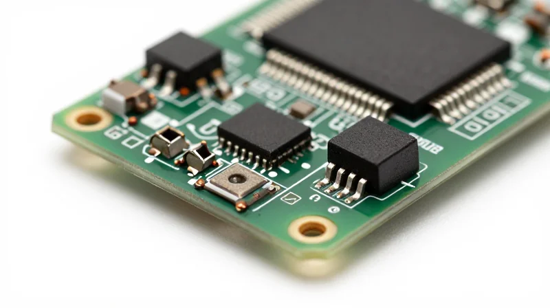
Selecting components for blood pressure sensors requires a balance between signal precision, power efficiency, and long-term environmental reliability. Given the sensitivity of pressure transducers, designers must prioritize components with low drift characteristics and high immunity to transient noise to ensure consistent diagnostic readings over the device lifecycle.
- Component Derating Protocols
Apply strict derating factors for capacitors and resistors to ensure operating conditions stay well below maximum thresholds, effectively mitigating stress-induced failures. - Humidity and Moisture Sensitivity
Utilize components rated for high-reliability medical environments (MSL Level 3 or better) to prevent ingress-related degradation during assembly and patient use. - Signal Integrity Balancing
Prioritize low-offset, low-drift operational amplifiers and high-precision reference voltages to minimize thermal noise floors in the sensor data acquisition chain.
Thermal Management in Enclosed Architectures
In miniature, enclosed medical housings, thermal management is constrained by the absence of active airflow. Design strategies must focus on conductive cooling paths to the enclosure walls or structural chassis to prevent thermal gradients that can induce measurement drift in the pressure transducer.
| Thermal Management Strategy | Implementation Detail | Impact on PCBA |
|---|---|---|
| Thermal Vias | Array of copper-filled vias under ICs | Distributes heat to ground planes |
| TIM Application | Phase-change materials between heat sources and case | Lowers junction temperature significantly |
| Copper Pours | Strategic use of thick-copper (2oz+) planes | Increases lateral heat dissipation area |
Best Practices for Thermal Simulation
To ensure reliable thermal performance, designers should perform finite element analysis (FEA) during the prototyping phase. By accurately modeling the ambient air pockets and material thermal conductivity within the housing, engineers can predict and resolve hotspots before reaching high-volume production, ensuring compliance with medical safety standards like IEC 60601-1.
Rigorous Validation and Testing Strategies
Multi-Stage Validation Framework
Validation of medical-grade sensor integration requires a multi-tiered approach that progresses from component-level verification to full-system clinical simulation. By identifying failure modes early, manufacturers can minimize rework and ensure the PCBA meets the stringent noise-to-signal ratios required for accurate blood pressure measurement.
| Testing Phase | Primary Objective | Clinical Relevance |
|---|---|---|
| In-Circuit Testing (ICT) | Verify connectivity and solder integrity | Prevent intermittent sensor signals |
| Functional Testing (FCT) | Validate electrical parameters of ADC output | Ensure raw data precision |
| Environmental Stress (ESS) | Test reliability under thermal/vibration load | Simulate real-world clinical use |
Key Performance Indicators (KPIs) for PCBA Testing
- Signal Stability
Measuring the drift of the pressure transducer output over extended periods to ensure it remains within the +/- 3mmHg clinical error threshold. - Noise Floor Analysis
Utilizing FFT analysis during testing to verify that the PCBA shielding effectively suppresses electromagnetic interference from surrounding circuitry. - Calibration Accuracy
Automated verification of the EEPROM stored calibration coefficients against controlled pneumatic pressure inputs.
Automated Test Pattern Implementation
def validate_pressure_range(sensor_output, expected_pascals, tolerance=0.01):
    error = abs(sensor_output - expected_pascals) / expected_pascals
    return error <= tolerance
By implementing automated test scripts like the one above, engineering teams can standardize the validation process. This ensures that every PCBA produced undergoes the same rigorous scrutiny, effectively eliminating human variability in the inspection of sensitive pressure-sensing nodes.
Mastering the design of blood pressure monitor PCBs is the foundational step in delivering clinical-grade accuracy to the healthcare market. By prioritizing signal integrity, adhering to strict DFM protocols, and ensuring EMC compliance, your engineering team can mitigate risks early in the development lifecycle. Ready to optimize your medical device performance? Contact our engineering consultancy team today to review your PCBA schematics and manufacturing strategy.
