
Engineering high-output audio within the constraints of a portable, compact chassis presents a unique set of challenges. As power density increases, thermal bottlenecks and signal interference threaten to degrade acoustic performance. This guide provides the expert framework needed to balance high-fidelity output with reliable, manufacturer-ready PCB design.
Understanding the Compact Audio Constraint
The Trilemma of Portable Audio Engineering
Designing a high-fidelity portable Bluetooth speaker PCBA requires balancing three competing constraints: physical footprint, thermal headroom, and electromagnetic compatibility. As chassis volumes shrink to prioritize portability, the proximity of the Class-D amplifier to sensitive signal processing components creates significant thermal density challenges. Effective layout optimization demands that engineers view the PCBA not merely as an electronic substrate, but as a critical thermal management component within the enclosure.
Thermal vs. Audio Fidelity Trade-offs
| Design Factor | Impact on Thermal | Impact on Audio Fidelity |
|---|---|---|
| Copper Weight | Higher weight improves heat spreading. | Minimal, if trace impedance is managed. |
| Component Density | Reduces airflow, increases hot spots. | Reduces board size, increases crosstalk. |
| Via Stitching | Conducts heat to inner planes/heatsinks. | Can disrupt ground planes if poorly placed. |
Frequently Asked Questions
- How does PCB thickness influence thermal performance?
Thicker boards (e.g., 1.6mm vs 0.8mm) offer more substrate material, but increased copper layering is more effective for lateral heat spreading, which is the primary requirement for compact speaker layouts. - Can I use the enclosure itself as a heat sink?
Yes, thermal interface materials (TIMs) can bridge the gap between the amplifier IC and the enclosure, though this must be balanced against mechanical vibration damping requirements to prevent acoustic rattles.
Component Placement Strategies for Signal Integrity

Signal Chain Floorplanning Fundamentals
Achieving optimal signal integrity requires a tiered approach to floorplanning, starting with the separation of sensitive analog audio stages from noisy digital switching power supplies. By utilizing a zoning methodology, designers can minimize crosstalk and inductive coupling that often degrade audio fidelity in high-density layouts.
Best Practices for Minimizing Noise and Ground Loops
- Analog-Digital Isolation
Strictly partition analog signal paths and digital control lines. Use separate ground planes joined at a single point to prevent high-frequency noise from corrupting the low-level audio signals. - Optimizing Return Paths
Keep the return paths for high-current amplifier stages short and direct to the local decoupling capacitors, preventing ground bounce that can introduce audible artifacts. - Class-D Switching Considerations
Place the output inductors as close to the Class-D amplifier IC as possible to minimize the area of the radiating antenna loop created by high-frequency switching edges.
| Component Group | Primary Constraint | Placement Priority |
|---|---|---|
| Bluetooth SoC | RF Interference | Isolated far from Class-D outputs |
| Power Stage (Amplifier) | Thermal/Current | Proximal to battery/DC-in with heat sinking |
| Analog Input/DAC | Signal Integrity | Away from switching regulators |
Mitigating Ground Loops in Compact PCBs
In portable audio devices, ground loops are often exacerbated by the return path through metallic chassis or shared interconnects. To mitigate this, prioritize a solid ground plane layer beneath all signal traces. For multi-layer designs, avoid splitting the ground plane underneath critical audio paths, as this forces return currents to take indirect routes, significantly increasing EMI and susceptibility to noise.
Thermal Management in High-Output Amplification
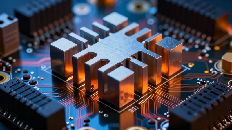
Thermal Management in High-Output Amplification
In high-output Class-D amplification, thermal performance is intrinsically linked to audio fidelity. As power density increases within constrained enclosures, heat buildup induces gain compression and potential thermal shutdown. Effective dissipation relies on turning the PCB itself into a heat spreader, utilizing copper geometry to manage heat flux away from sensitive switching stages.
Optimizing Thermal Dissipation Pathways
Designers should prioritize the following structural optimizations to mitigate localized hot spots:
- Thermal Vias
Utilize a dense array of plated through-hole vias under amplifier ICs to create a low-impedance path to inner ground planes, which act as large-scale radiators. - Copper Pours
Maximize top and bottom copper pour areas connected to power ground, ensuring these are not isolated by signal traces to maintain a continuous thermal mass. - Heatsink Integration
For extreme power density, implement direct thermal bonding using high-conductivity pads between the IC package and an external aluminum chassis component.
Comparison of Thermal Mitigation Techniques
| Technique | Primary Benefit | Implementation Complexity |
|---|---|---|
| Thermal Vias | Vertical heat transfer | Low |
| Extended Copper Pours | Lateral heat spreading | Low |
| Direct Chassis Coupling | Max dissipation/Heat sinking | High |
Frequently Asked Questions
- How many thermal vias are enough?
A common rule of thumb is a 3x3 or 4x4 grid under the thermal pad of the amplifier, with 0.3mm drill diameters, ensuring they are filled to minimize air gaps. - Does solder mask thickness affect cooling?
Yes; standard solder mask acts as an insulator. Avoid covering high-heat-dissipation areas with solder mask if possible, or ensure it is as thin as the process allows.
Optimizing Power Delivery Networks (PDN)
Minimizing Impedance for High-Current Transients
Effective PDN design for portable speakers requires minimizing the loop inductance between the battery/DC-DC converter and the amplifier IC. In high-output Class-D designs, sudden current spikes can trigger voltage dips that degrade audio fidelity and introduce audible ripple noise. Designers must utilize wide, short traces and multi-layer power planes to keep impedance low, ensuring the amplifier maintains a stable voltage rail even during peak bass output.
PDN Component Selection Criteria
| Component | Role in PDN | Design Optimization |
|---|---|---|
| Bulk Capacitors | Energy Storage | Low ESR/ESL placement near output stage |
| Decoupling Caps | High-Frequency Noise Filtering | Minimize parasitic inductance with 0201/0402 footprints |
| Ferrite Beads | EMI/Ripple Suppression | Series placement between power rails and sensitive stages |
Frequently Asked Questions on PDN Integrity
- How do I prevent ripple noise from reaching the pre-amplifier?
Implement separate analog and digital power planes, utilizing a star-grounding configuration to ensure noise generated by the Class-D power stage does not bleed into the sensitive signal path. - What is the impact of via stitching on PDN stability?
Via stitching reduces the path of least resistance for return currents. By placing thermal vias in a dense array near the amplifier, you lower both the DC resistance and the parasitic inductance of the power delivery path.
Layout Best Practices
To achieve optimal performance, avoid routing high-current paths through narrow bottlenecks. Instead, dedicate entire internal layers to the power plane if board space permits. If restricted, ensure that the return path remains uninterrupted under the power-carrying traces, as any gap in the ground plane will drastically increase loop area and EMI emissions.
DFM: Bridging Design and Mass Production
Bridging Design for Manufacturing (DFM) and Scale
Translating a thermally optimized layout into a mass-produced assembly requires strict adherence to fabrication and assembly constraints. While a board might perform flawlessly in the lab, its manufacturability depends on panelization efficiency, solder paste stencil thickness, and tolerance stack-ups that impact thermal path integrity.
Critical DFM Metrics for High-Density Audio Boards
| DFM Constraint | Reasoning for Audio PCBA | Manufacturing Impact |
|---|---|---|
| Via-in-Pad | Reduces thermal path length to ground planes | Requires filled/capped vias to prevent solder wicking |
| Copper Weight | Supports high-current delivery for Class-D amps | Higher weight (2oz+) increases etch time and costs |
| Component Clearance | Allows for automated optical inspection (AOI) | Reduces false defect reports during mass production |
Common DFM Challenges and Solutions
- How does panelization affect thermal layout?
Improper panelization can lead to uneven thermal dissipation during reflow, resulting in warped boards. Always prioritize symmetrical component placement to maintain thermal mass balance across the panel. - Why is thermal via placement sensitive to assembly?
If thermal vias are placed too close to sensitive high-impedance traces without adequate solder mask damming, solder migration can create electrical shorts. Use plugged or masked vias to ensure consistent thermal conductances. - Does copper pour density impact wave soldering?
Excessive continuous copper pours can act as heat sinks during selective soldering, causing cold solder joints. Implement thermal reliefs for all pads connected to large planes to ensure consistent wetting.
Design Verification Workflow
To ensure design intent survives the factory floor, implement a rigorous Design for Assembly (DFA) review. Use the following snippet as a checklist for final pre-production validation:
1. Verify Thermal Relief: Ensure all ground-plane connections use 4-spoke thermal reliefs.
2. Check Fiducials: Verify three global fiducials on the board and panel rail.
3. Validate Solder Mask: Check for 0.1mm expansion on all high-current vias.
4. Confirm Clearance: Ensure 0.5mm clearance between power traces and thermal heatsink attachment points.
Minimizing Electromagnetic Interference (EMI)
Strategic Partitioning and Shielding
To prevent interference between high-frequency Bluetooth transceivers and high-current audio amplification stages, board layout must prioritize physical isolation. Separating the radio frequency (RF) front-end from the switching noise of Class-D amplifiers is critical. Utilizing grounded copper keep-out zones and dedicated shielding cans for the Bluetooth module acts as the first line of defense against radiated emissions.
Key Mitigation Strategies
- RF Trace Routing
Keep RF traces on the top layer with a solid ground plane directly underneath to minimize impedance discontinuities and loop area. - Component Isolation
Maintain a minimum distance of at least 10mm between the antenna feed point and any high-frequency switching components or inductors. - Ground Plane Integrity
Use a continuous ground plane; avoid splitting planes under sensitive analog circuits, as this creates parasitic inductance and exacerbates EMI.
Managing Switching Noise and Crosstalk
The switching frequency of the Class-D audio amplifier creates high-order harmonics that can couple into the Bluetooth antenna trace. Implementing proper decoupling and layout-level filtering is essential for maintaining a high signal-to-noise ratio.
| EMI Source | Impact | Mitigation Technique |
|---|---|---|
| Class-D Switching | Broadband Noise | Ferrite beads and snubber circuits |
| Inductor Radiation | Coupling to RF traces | Shielded inductors and 90-degree orientation |
| Data Line Noise | Jitter/Data errors | Differential pair length matching |
/* Example of stitching via placement for edge EMI containment */
const viaStitch = {
  pitch: '2.5mm',
  clearanceToTrace: '0.5mm',
  purpose: 'Ground-plane-to-enclosure-shielding'
};
Verification and Prototyping Procedures
Thermal Validation Protocols
Prototyping must include stress testing under worst-case thermal scenarios to ensure the Class-D amplifier and Bluetooth SoC remain within operating limits. Initial validation requires long-duration high-output sweeps to saturate the system's thermal capacity. Use high-resolution thermal imaging to identify 'hot spots' on the PCBA, specifically focusing on the power stage MOSFETs and voltage regulators.
| Test Phase | Target Component | Verification Metric |
|---|---|---|
| Steady-State Analysis | Class-D Amplifier | Max Junction Temperature |
| Transient Response | Power Regulators | Voltage Ripple/Droop |
| Environmental Soak | RF/SoC Shielding | Signal Integrity/Packet Loss |
Acoustic Sweep and EMI Integration
Thermal dissipation solutions must not compromise the acoustic integrity of the chassis or the EMI profile of the PCBA. Acoustic sweep testing should be performed in conjunction with thermal monitoring to ensure that high temperatures do not induce frequency response shifts or non-linearities in the signal chain. If a heat spreader or thermal pad is adjusted, a full re-run of the EMI compliance scan is required to ensure no radiated emissions have spiked due to the mechanical change.
Verification FAQ
- How long should a thermal stress test run?
Run the device at maximum continuous output power until the junction temperature stabilizes, typically requiring 30 to 60 minutes of operation. - What tools are essential for prototyping?
A high-resolution infrared camera, a multi-channel data logger, and a spectrum analyzer for monitoring EMI during thermal load cycling are non-negotiable. - Does thermal adhesive impact impedance?
Poorly applied thermal interface materials can introduce parasitic capacitance, potentially affecting high-speed Bluetooth trace impedance; always verify signal integrity after mechanical assembly.
By rigorously applying these PCB layout strategies, you can successfully overcome the thermal and signal hurdles inherent in compact audio design. Precision in your layout stage ensures professional-grade acoustic quality and long-term product reliability. Ready to elevate your hardware project? Contact our engineering team today to discuss your next high-performance audio design.
