
In the high-stakes world of medical diagnostics, a delay in production or a field failure is more than just a business setback—it’s a risk to patient health. Mastering Design for Manufacturing (DFM) is the difference between a prototype that stalls and a product that scales. This guide provides the technical framework for optimizing your blood glucose meter PCBA for speed, reliability, and cost-efficiency.
The Fundamentals of DFM in Medical Electronics

The Strategic Importance of DFM in Diagnostic Hardware
Design for Manufacturing is not merely a cost-reduction strategy; it is a fundamental requirement for ensuring the regulatory compliance and long-term reliability of life-critical diagnostic hardware. In blood glucose meters, where the device must operate with high precision under varying environmental conditions, DFM integrates manufacturing constraints directly into the PCB design phase to prevent production defects, minimize assembly errors, and ensure consistent signal integrity.
Key DFM Objectives for Medical PCBs
- Design Standardization
Utilizing standard component libraries and panelization techniques to reduce lead times and improve throughput during automated surface mount assembly. - Process Robustness
Selecting materials and stack-ups that withstand multiple thermal cycles, ensuring the meter remains accurate after prolonged usage and potential sterilization processes. - Cost Efficiency
Optimizing trace widths, via structures, and board finish specifications to lower fabrication costs without compromising the high-impedance paths required for glucose sensing.
DFM Considerations: Prototype vs. Production
| Feature | Prototype Focus | High-Volume DFM Focus |
|---|---|---|
| Component Selection | Availability and Speed | Cost, Lead Time, and Reliability |
| PCB Panelization | N/A (Single Board) | Optimization for Fab/Assembly Yield |
| Tolerance Analysis | Functional Verification | Worst-Case Circuit Analysis (WCCA) |
| Test Strategy | Manual Probing | Bed-of-Nails or Flying Probe |
Addressing Design Integrity
When moving from schematic to layout, engineers must prioritize testability and component accessibility. Implementing Design for Test (DFT) alongside DFM allows for rapid fault detection during manufacturing, which is essential when handling medical-grade electronics where quality assurance benchmarks are strictly monitored by regulatory bodies like the FDA or EMA.
Optimizing Board Layout for Miniaturization

Strategies for High-Density Interconnect (HDI) Integration
Miniaturizing blood glucose meters necessitates shifting from standard through-hole construction to sophisticated HDI manufacturing techniques. By utilizing microvias, blind and buried vias, and finer trace/space geometries, designers can drastically reduce the board footprint while increasing component density. However, these techniques require strict adherence to fabrication tolerances to avoid yield-crushing defects like microvia barrel cracking or registration errors.
| Feature | Standard PCB | HDI PCB |
|---|---|---|
| Via Type | Through-hole | Microvia (Laser Drilled) |
| Trace/Space | 6/6 mil | 2/2 mil - 3/3 mil |
| Component Density | Low to Moderate | Very High |
| Layer Count | 2-4 Layers | 6+ Layers (Build-up) |
Maintaining Signal Integrity in Compact Environments
Reducing physical space brings conductors closer together, increasing the risk of crosstalk and electromagnetic interference (EMI). In glucose meter designs—which often incorporate sensitive analog sensing circuits alongside high-speed digital processing—effective isolation is paramount. Employing differential signaling for sensitive sensor lines and maintaining continuous reference planes beneath high-speed signals are critical DFM measures to preserve signal integrity without sacrificing area.
Frequently Asked Questions: HDI Design for Medical Devices
- When is HDI necessary for medical devices?
HDI becomes necessary when the form factor requirement forces a component density that cannot be achieved with standard through-hole vias or when specific signal routing requires high-density trace escape patterns that consume too much board area. - Does HDI increase the cost per unit?
While HDI technology increases the cost per board due to more complex manufacturing processes (laser drilling, sequential lamination), it often reduces total cost by allowing for smaller, more efficient enclosures and reduced system-level complexity. - How does via-in-pad affect assembly reliability?
Via-in-pad technology is crucial for miniaturization; however, it requires the vias to be capped and plated over (IPC-4761 Type VII) to prevent solder wicking and ensure reliable attachment of fine-pitch components.
Component Selection Strategies for Supply Chain Resilience
Component Selection Strategies for Supply Chain Resilience
In the medical device industry, selecting the right components is as much about lifecycle management as it is about electrical specifications. To ensure blood glucose meters remain cost-effective and manufacturable over a multi-year product lifecycle, engineers must prioritize parts with high supply chain visibility and avoid components nearing end-of-life (EOL) status.
Risk Mitigation Framework
| Strategy | Design Impact | Supply Chain Benefit |
|---|---|---|
| Multi-source sourcing | Higher footprint flexibility | Reduced reliance on single vendors |
| Standardized packages | Simplified PCB assembly | High availability from multiple distributors |
| Lifecycle monitoring | Proactive component audits | Early detection of EOL notifications |
Best Practices for Component Selection
- How do I evaluate long-term availability?
Utilize component lifecycle databases like SiliconExpert or IHS Markit to track the maturity stage of integrated circuits and critical analog components before finalizing your Bill of Materials. - Why prefer common package footprints?
Selecting standard footprints (e.g., 0402 or 0603 passives) allows for rapid procurement from secondary suppliers if your primary vendor faces inventory shortages. - What is the danger of cutting-edge niche parts?
While innovative, boutique sensors or microcontrollers often suffer from shorter lifecycles and limited supply channels, increasing the risk of expensive mid-lifecycle board re-spins.
Ultimately, a resilient design minimizes the use of proprietary components that cannot be easily substituted. By implementing a 'Design for Availability' philosophy, firms protect their margins and ensure patients have uninterrupted access to diagnostic technology.
Managing Thermal Dynamics in Handheld Diagnostics

Thermal Dynamics in Handheld Diagnostics
Managing thermal loads in handheld blood glucose meters requires a holistic approach that balances component heat dissipation with the constraints of a small, enclosed chassis. Excessive heat drift can directly impact the analog front-end (AFE) accuracy of enzymatic glucose sensors, making isothermal design a top priority.
Key Strategies for Heat Dissipation
- Optimized Copper Pouring
Utilize dedicated ground planes as thermal spreaders to pull heat away from the processor and power management ICs toward cooler areas of the board. - Strategic Component Placement
Keep heat-generating components such as power regulators away from the sensitive analog measurement circuitry to prevent thermal gradients from affecting sensor calibration. - Thermal Vias and Pads
Implement arrays of thermal vias under power-intensive chips to conduct heat directly to the bottom layer or internal ground planes, significantly lowering junction temperatures.
Thermal Management Techniques Comparison
| Technique | Implementation Difficulty | Thermal Impact |
|---|---|---|
| Copper Pour Spreading | Low | Moderate |
| Thermal Vias | Medium | High |
| Active Cooling (Fan/Peltier) | Very High | Maximum |
Frequently Asked Questions
- Does thermal drift impact sensor accuracy?
Yes, variations in ambient temperature on the PCB can induce errors in the electrochemical readings of a glucose strip, necessitating robust thermal decoupling. - Are heat sinks recommended for handheld devices?
Traditional finned heat sinks are usually impractical; designers should instead leverage PCB-integrated solutions like high-conductivity copper pours and thermal interface materials (TIMs).
Stack-up Design and Impedance Control
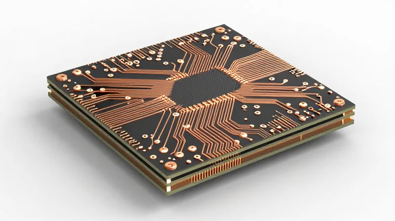
Strategic PCB Layer Stack-up for Precision Diagnostics
For blood glucose meters, the PCB stack-up serves as the foundation for both signal integrity and EMI suppression. Given that glucose sensors operate with low-level microampere currents, the board must prioritize a low-noise environment. A minimum four-layer stack-up is recommended, utilizing internal ground planes to shield high-frequency clock signals from sensitive analog traces. By positioning signal layers adjacent to solid reference planes, you ensure a continuous return path, significantly reducing loop inductance and crosstalk.
Impedance Control and Signal Integrity
Precision impedance control is not merely for high-speed digital buses but is critical for the sensor interface to prevent signal reflections. Whether the meter utilizes a proprietary serial protocol or standard I2C, maintaining a 50-ohm characteristic impedance is vital for signal consistency.
| Parameter | Design Rule | Impact on Performance |
|---|---|---|
| Trace Impedance | 50 Ohm (+/- 10%) | Reduces signal reflection and noise |
| Layer Symmetry | Balanced stack-up | Prevents board warping during reflow |
| Reference Plane | Solid Ground (GND) | Minimizes EMI and return loop area |
Frequently Asked Questions on Stack-up DFM
- Why is a four-layer board superior to a two-layer for glucose meters?
A four-layer board allows for dedicated power and ground planes, which provide essential shielding and decoupling, reducing the noise floor that could otherwise interfere with electrochemical sensor readings. - How does dielectric thickness affect my design?
The distance between the signal layer and the ground plane determines your trace width requirements for impedance control; thinner prepreg materials facilitate smaller trace widths suitable for HDI designs. - Is impedance control expensive?
While it requires specific manufacturing controls and TDR testing, it is cost-effective when it prevents the need for board spins caused by unreliable connectivity or poor sensor sensitivity.
Design for Test (DFT) Methodologies
Effective DFT for medical diagnostics requires a strategic balance between test coverage and physical space constraints. By prioritizing test point accessibility and logical partitioning, engineers can achieve higher first-pass yields while minimizing the time-to-market for portable blood glucose meters.
Comparative Analysis: ICT vs. Flying Probe
| Feature | In-Circuit Testing (ICT) | Flying Probe Testing |
|---|---|---|
| Test Speed | High (Parallel testing) | Low (Sequential testing) |
| Fixture Cost | High (Custom bed-of-nails) | Low (Fixtureless) |
| Board Space | High overhead | Minimal impact |
| Flexibility | Low (Changes require new fixture) | High (Software-driven) |
Implementation Best Practices for Diagnostic Reliability
- Standardize Test Point Geometry
Utilize circular test pads with a minimum 0.035-inch diameter, placed on a 0.100-inch grid whenever possible to simplify fixture alignment and improve probe contact reliability. - Strategic Node Partitioning
Isolate high-precision analog sensing circuits from noisy digital processing blocks using jumpers or isolation resistors, allowing for targeted functional testing without interference. - Avoid Via Probing
Probing vias can lead to solder cracking and intermittent failures; always provide dedicated landing pads for probe access to maintain board integrity. - Boundary Scan (JTAG) Integration
Leverage IEEE 1149.1 JTAG standards to test complex IC connectivity and internal registers without requiring physical access to every individual signal trace.
Managing Thermal and Signal Integrity in Testing
When implementing test access, ensure that test pads are not placed in the immediate path of sensitive analog return currents for the glucose sensor. Additionally, maintain adequate clearance between test points to prevent accidental shorts during the testing process, which is especially vital given the high sensitivity of blood glucose monitoring hardware.
Surface Finish and Material Selection
Strategic Material Selection for Medical Reliability
For portable medical devices like blood glucose meters, the PCB substrate must maintain structural integrity under frequent thermal cycling and mechanical stress. Standard FR-4 is often insufficient due to high thermal expansion coefficients that can induce micro-cracks in sensitive solder joints. Instead, high-Tg (glass transition temperature) materials are recommended to ensure dielectric stability during the heat-intensive soldering process and subsequent operational use.
| Material Type | Primary Advantage | Best Use Case |
|---|---|---|
| Standard FR-4 | Low cost | Non-critical, consumer-grade items |
| High-Tg FR-4 | Thermal stability | Medical handheld monitoring devices |
| Polyimide | Flexibility & Heat resistance | Small, dense sensor-integrated circuits |
Surface Finish Optimization: Balancing Solderability and Longevity
Surface finishes directly influence the PCB's shelf life, solder joint reliability, and ability to withstand humid or clinical environments. While HASL is cost-effective, its uneven surface is unsuitable for the fine-pitch components often found in modern glucose meter chipsets. Electroless Nickel Immersion Gold (ENIG) is the gold standard for these applications due to its excellent flatness and oxidation resistance.
- Why is ENIG preferred over HASL for medical sensors?
ENIG provides a perfectly planar surface essential for fine-pitch BGA or CSP components and offers superior corrosion resistance compared to lead-free HASL. - Can OSP (Organic Solderability Preservative) be used in medical applications?
OSP is cost-effective but sensitive to multiple reflow cycles and environmental storage; it is typically avoided for high-reliability medical devices requiring long-term durability. - How does material selection affect signal integrity?
Selecting materials with a stable dielectric constant (Dk) ensures that the high-frequency signals used in glucose monitoring maintain impedance consistency across varying temperature ranges.
Verification and Validation: The Path to Regulatory Compliance
Integrating Regulatory Compliance into the DFM Workflow
Regulatory compliance is not a final checkpoint but a continuous design objective that must be woven into every DFM decision. By prioritizing traceability, thermal stability, and contamination control during the design phase, manufacturers can preemptively address the rigorous documentation requirements set forth by the FDA and ISO 13485 standards.
Critical DFM Factors Influencing Certification
| DFM Focus Area | Regulatory Impact | Compliance Benefit |
|---|---|---|
| Material Selection | Biocompatibility (ISO 10993) | Prevents toxic leaching and ensures safety. |
| Traceability | Device History Record (DHR) | Facilitates root cause analysis and audit logs. |
| Component Derating | Reliability/Risk Management | Reduces failure rates under environmental stress. |
Validation and Verification (V&V) Efficiency
Verification proves that the PCB meets the specified requirements, while validation confirms that the blood glucose meter functions safely in the hands of the end-user. DFM decisions that standardize test points and facilitate non-destructive inspection accelerate the V&V cycle, significantly reducing time-to-market without compromising safety.
- How does DFM support FDA audit readiness?
DFM creates a standardized, predictable process that provides clear documentation regarding component sourcing and manufacturing tolerances, which is essential for proving design control compliance. - Why is material selection critical for regulatory approval?
Medical devices must adhere to strict biocompatibility standards; selecting substrates with verified material certificates simplifies the certification process and ensures long-term sensor reliability. - Can DFM reduce the cost of V&V testing?
Yes, by integrating Design for Test (DFT) strategies, you eliminate the need for custom, complex test fixtures, thereby streamlining the validation process and lowering capital expenditure.
By adhering to these rigorous DFM principles, engineering teams can significantly reduce production rework and achieve faster time-to-market for medical diagnostic devices. Are you ready to optimize your next design? Contact our engineering team today for a comprehensive DFM audit of your current project.
