RF PCB design isn't some mysterious black art, but there are plenty of details that can trip you up. From 2.4G to 28GHz millimeter-wave projects, every board reinforces one truth: details make the difference.
Industry data confirms the trend. China's high-frequency and high-speed PCB market reached RMB 21.2 billion in 2024 and is projected to exceed RMB 30 billion by 2026, with annual growth exceeding 18%. Demand is strong, but engineers who can truly deliver quality RF PCB designs remain scarce.
The core challenges of RF design come down to a few key areas: precise impedance control, effective isolation, proper thermal management, and the right material selection. Each directly impacts final performance. At 28GHz, standard FR-4 loses 2-3dB/cm, while PTFE materials can achieve below 0.3dB/inch — a dramatic difference.
In RF PCB design, layout sets the foundation. If the foundation is weak, even the best routing won't save the design.
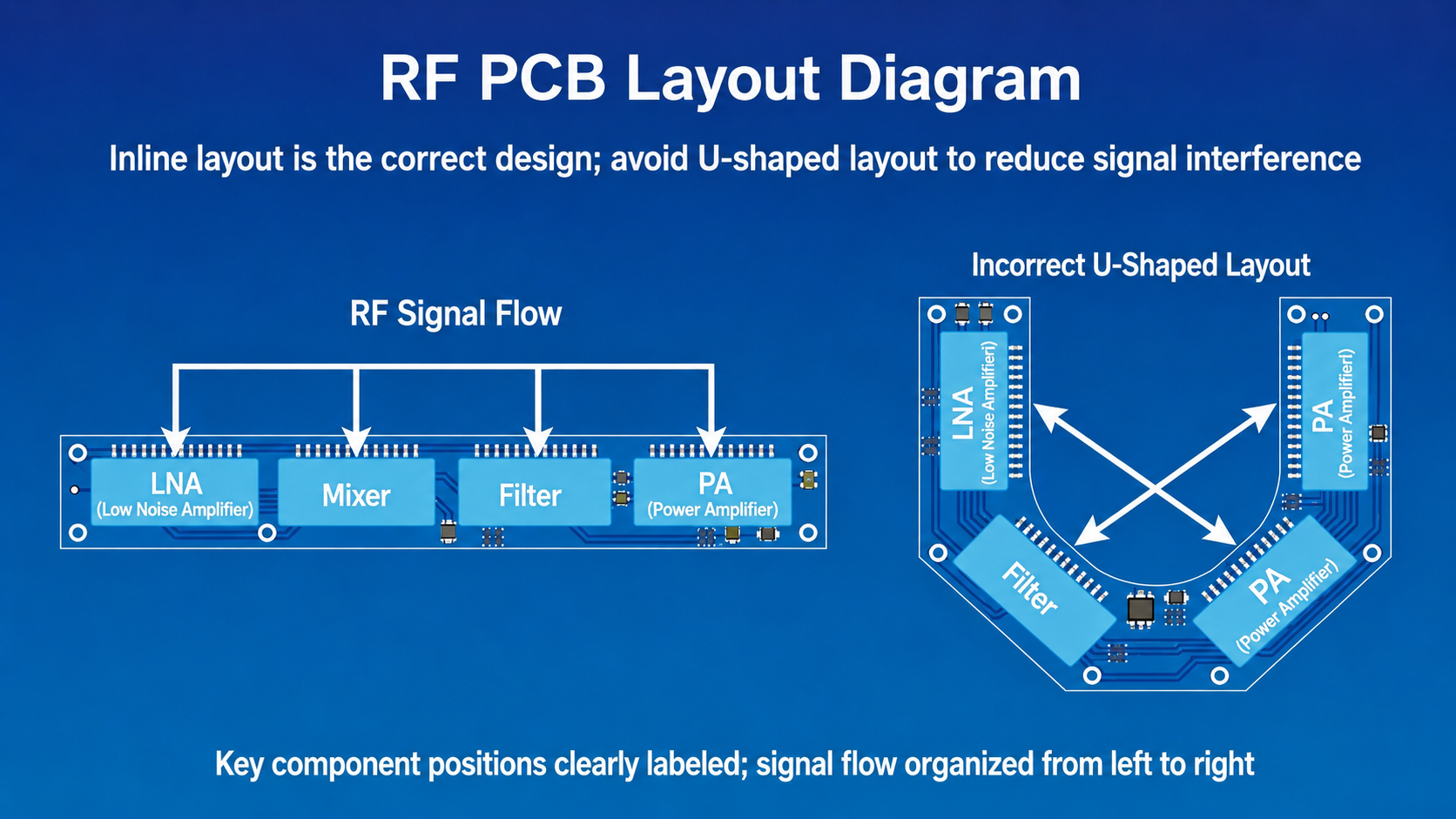
Place RF signals in a straight line from input to output, minimizing bends and crossings to reduce signal interference. One dual-channel power amplifier project initially placed two channels side by side to save space — intermodulation performance failed to meet specifications. After switching to an inline layout, the metrics passed immediately.
Multi-channel designs require millimeter-level precise symmetry — component placement, trace lengths, and via positions must be consistent to maintain phase and amplitude matching. In phased array antenna designs, channel phase differences exceeding 10° noticeably degrade beamforming performance.
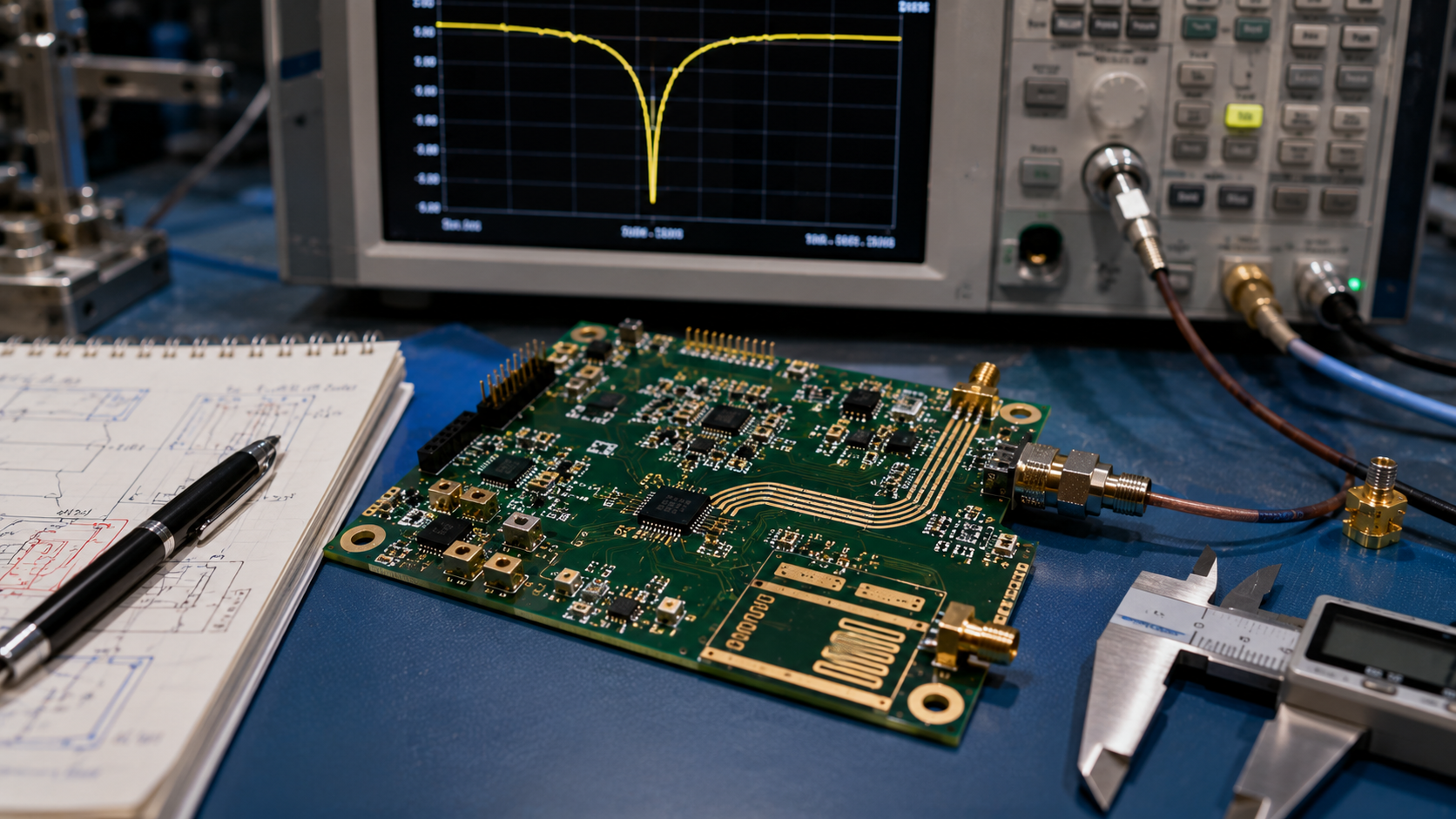
Know which traces carry RF signals, which carry control signals, and which are power — before placing a single component. Sketching a signal flow diagram on paper first helps avoid routing dead-ends later.
Place high-power inductors near board edges or with added copper for heat dissipation
Place RF matching inductors close to their corresponding components to minimize parasitic inductance
Orient adjacent inductor magnetic cores perpendicular to each other to reduce mutual coupling
In one 5G base station power amplifier project, two matching inductors placed in parallel created a resonance at 3.5GHz, dropping efficiency by over 1 percentage point. Rotating the inductors 90° solved the problem.
Separate high-power circuits (power amplifiers, switches) from low-noise circuits (LNAs, mixers) with sufficient distance — at least 5mm — and use ground copper or shielding walls between them. Add metal shielding cans where necessary.
High-performance RF boards typically use shielding cavities to isolate functional regions. Key design considerations:
Cavity height: Balanced — too low restricts heat dissipation, too high increases cost
Grounding vias: Place one every λ/10 (λ = wavelength at operating frequency)
Apertures: Keep them as small as possible to minimize electromagnetic leakage
Shape: Regular shapes only — avoid sharp corners and narrow gaps (corners concentrate electric fields; gaps create slot antennas)
Size: Avoid operating frequency resonance points
Once layout is done, routing is the critical phase that determines final performance.
RF signal traces must be designed with 50Ω impedance control — adjusting trace width, dielectric thickness, and copper thickness accordingly. Use impedance calculation software rather than relying on experience. Most PCB manufacturers offer ±5% impedance control, with leading suppliers achieving ±3%.
Key point: Vias, test points, and pads all affect impedance. Vias introduce parasitic inductance and capacitance, creating impedance discontinuities. If vias are unavoidable, use back-drilling to remove stubs or use multiple parallel vias to reduce impedance.
Maintain trace spacing of at least 3× trace width (5× or more for high-frequency bands)
Avoid excessive vias — each via introduces a discontinuity point
Use surface traces whenever possible; prefer back-drilled or blind/buried vias when necessary
Keep RF zones, digital zones, and power zones physically separated. Use ground copper isolation between regions and dedicate separate power filtering. One design ran a clock trace directly under an RF chip, raising the board's noise floor by 10dB.
Ground return paths in high-power areas must be short and wide. Use 8-12 vias on power amplifier ground pads to ensure low-impedance grounding. Use 2oz or heavier copper for ground planes to reduce impedance and improve heat dissipation.
For transceiver designs, physically separate transmit and receive channels — use different layers or shielding walls. One Bluetooth module project failed transmit power and receive sensitivity specifications because the PA and LNA were too close; transmit signals coupled into the receive path, degrading sensitivity by 20dB. Separating the two modules and adding a shielding wall resolved the issue.
Keep sensitive signals like clock and reset lines away from RF traces. Best practices:
Route them on inner layers with ground copper shielding above and below
Surround with continuous ground planes
Add shielding cans when necessary
Remove floating copper — either ground it or eliminate it completely to avoid antenna effects
Avoid narrow slots in ground copper — they radiate at high frequencies
Use rounded corners instead of sharp corners; use multiple small vias instead of one large one
Keep metal, components, and traces clear of the antenna area. Maintain clearance (at least λ/4). Ensure uniform dielectric material near the antenna — avoid abrupt Dk changes that affect performance.
Understanding the underlying physics helps you generalize and adapt to various scenarios.
Higher frequency means shorter wavelength — and greater sensitivity to geometry. At 28GHz, wavelength is only 10.7mm. A 10mm trace approaches one wavelength, and both trace geometry and surrounding media produce significant effects.
Impedance control reduces signal reflection. When impedance mismatches, signal energy reflects back to the source, increasing VSWR and reducing power transfer efficiency. At 28GHz, a single right-angle bend can introduce extra capacitance equivalent to 20% of trace width — enough to break impedance continuity.
Isolation prevents crosstalk and self-oscillation. RF signals readily couple through space, ground loops, and power supply paths. High-power amplifier harmonics coupling directly into an LNA input can overwhelm weak received signals.
Material selection is decisive. FR-4 shows significant loss above 1GHz, with Dk variation of ±10% across frequency. High-frequency materials like Rogers 4350B maintain Dk stability within ±0.05 and loss factor below 0.003 — at 5-8× the cost of FR-4, but essential at high frequencies. Hybrid stackups — high-frequency materials for RF layers and FR-4 for others — are now common, balancing performance and cost.
Thermal management is often underestimated. RF devices are inefficient — most input power converts to heat. One power amplifier reached 125°C after 5 minutes at full power, compressing gain by 3dB and dropping efficiency by 5 percentage points. Adding copper heatsinks and thermal vias dropped the temperature to 85°C and stabilized performance.
RF PCB design is a specialized skill, but it's not out of reach.
Start at lower frequencies. Master the basics at 2.4G or 5.8G before tackling millimeter-wave design. Lower frequencies offer larger design margins and more room for error.
Study proven examples. Examine how successful designs handle layout, routing, and detail. Reference designs from datasheets — understand why every trace and via is where it is.
Use simulation tools. ADS, HFSS, and similar tools catch issues early. Run transmission line simulations before routing and full-board EM simulations after routing. Results may differ from measurements, but trends are reliable.
Iterate frequently. RF design is an iterative process. Build a working version, test it, identify problems, and optimize. Each iteration brings improvement. One project took five revisions to meet specifications — but each version improved, and the final board passed all tests on the first formal submission.
Learn from others. Discussing problems with experienced designers helps you avoid common mistakes.
RF PCB design has no shortcuts — it's about practice, thought, and learning from experience. Industry data shows fewer than 100 service providers in China capable of full-process high-frequency high-speed PCB design; only about 30% can reliably deliver designs with signal rates above 25Gbps. Mastering RF PCB design is mastering a scarce and valuable skill.
Reading about it isn't enough — you have to build boards. Pick up your EDA tool and start your RF design journey today.
Need RF PCB Design and Manufacturing Support?
AnyPCBA has extensive experience in RF PCB design and manufacturing, covering projects from 2.4G to millimeter-wave frequencies. Our capabilities support 2-64 layers, including high-frequency hybrid (Rogers + FR-4), HDI, rigid-flex, and more — meeting the demanding requirements of RF PCB design.
Our engineering team provides DFM design reviews before production, helping you identify potential issues in layout, impedance, and material selection — especially critical in high-frequency, high-density RF designs.
Contact us to discuss your project →