Introduction: PCB warpage and bowing are among the most common hidden defects in SMT production. They can cause placement offset, poor solder joints, cracked components, and AOI failures. This article explains the causes—thermal, plating, material, design, and mechanical—and the measures to prevent them.
Description: Based on AnyPCBA's small-to-medium volume PCB and PCBA manufacturing experience, this guide explains the causes of PCB warpage and bowing—from thermal expansion and uneven plating to asymmetric stack-ups and material selection—and how DFM review and process control can prevent these issues before production.
PCB warpage and bowing are among the most common hidden defects in SMT production. They can cause placement offset, poor solder joints, cracked components, and even prevent an entire batch from passing AOI inspection.
What makes it more complicated: warpage is rarely caused by a single factor. It results from the combined effects of temperature, material, plating, processing, and design. This article examines the causes from the manufacturing side and the measures to prevent them.
Temperature changes cause PCB thermal expansion or contraction. If the two sides of the board are not exposed to the same thermal influence, the board bends or warps.
This is especially common during lamination and reflow. During lamination, if the top and bottom heating plates are not uniform in temperature, the core and prepreg shrink at different rates, resulting in warpage. During reflow, uneven heating produces similar problems.
Uneven plating can cause thicker copper on one side of the board and thinner copper on the other. Since copper and substrate have very different CTEs, uneven copper thickness amplifies this difference and causes deformation.
If PCB thickness is not uniform, the board may bend or warp. This can result from material variation or pressure variation during production.
If PCB dimensions are incorrect, the board may bend or warp. This can result from design errors or manufacturing process deviations.
If component soldering on the board is uneven, the board may bend or warp. This can result from manufacturing errors or assembly process issues.
Low-quality substrates may cause warpage or bowing. This can result from material defects or quality issues during production.
If processing deviations are too large, the board may bend or warp. This can result from processing errors or machine failure.
The PCB material may not be suitable for manufacturing requirements, causing warpage. For example, CTE mismatch or insufficient Tg to support subsequent processes.
Design issues can cause warpage. Common causes include unbalanced copper distribution, asymmetric stack-up, and unreasonable panelization.
During transport, installation, or use, mechanical stress can cause PCB bending or warping.
To prevent PCB warpage and bowing, the following measures should be taken:
Select board thickness and dimensions based on actual requirements, ensuring the board can withstand expected loads without excessive bending or warping.
During PCB manufacturing, ensure plating uniformity to avoid thicker copper on one side and thinner on the other, which causes warpage.
During PCB processing, strictly control deviations to ensure board dimensions and shape meet design requirements and avoid excessive bending or warping.
During PCB design and assembly, arrange component positions and spacing reasonably to avoid uneven distribution on the board, which can cause warpage.
During PCB soldering, control soldering temperature and time to avoid overheating or excessive heating time, which causes warpage.
During PCB use and storage, monitor temperature changes to avoid uneven thermal influence on different sides of the board, which causes warping.
During PCB design and assembly, add support structures to enhance board rigidity and prevent warping.
During PCB design and assembly, add frames or edges to enhance board stability and rigidity and prevent warping.
As a factory focused on small-to-medium volume PCB and PCBA manufacturing, AnyPCBA has accumulated years of experience in warpage control.
Our manufacturing capabilities cover 2 to 64 layers, including HDI, rigid-flex, and high-frequency hybrid. We hold ISO 13485 (medical) and IATF 16949 (automotive) certifications.
For warpage issues, our DFM review and production control focus on:
Design side:
Copper balance: avoiding large copper areas coexisting with empty areas
Stack-up symmetry: asymmetric stack-ups are a primary cause of lamination warpage
Panelization: whether rail width and depaneling method affect rigidity
Board thickness and dimensions: thin boards and large boards are more prone to warping
Manufacturing side:
Lamination parameters: temperature uniformity, pressure uniformity, ramp rates
Plating uniformity: copper thickness tolerance, pattern distribution effects
Material selection: choosing appropriate Tg and CTE substrates based on thickness and layer count
Cooling and storage: cooling rate after lamination, storage environment temperature and humidity control
Inspection side:
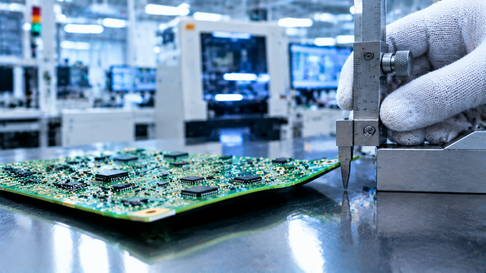
Warpage measurement: standard boards controlled between 0.70% and 0.75%, BGA boards within 0.5%
Pre-reflow check: confirming warpage is within acceptable range before SMT
Post-solder check: confirming no deformation from stress release after soldering
Our engineers help you anticipate warpage risks at the design stage, so your boards are not only buildable, but pass through the SMT line reliably.
If you're working on PCB design, or have encountered warpage issues, contact us through our website.
What warpage issues have you encountered in your projects? Share your experience in the comments.