
Introduction: Vias are essential to PCB layout, connecting traces across layers and delivering power throughout the board. This article covers traditional through-hole vias, blind and buried vias, microvias, annular ring requirements, aspect ratios, and how to manage via rules effectively in modern PCB design.
Description: Based on AnyPCBA's small-to-medium volume PCB manufacturing experience, this guide explains via design rules from standard through-holes to microvias, and how DFM review can help engineers catch via-related manufacturing risks before production.
A PCB may contain thousands of traces, pads, and vias, used to route signals and deliver power between component pins. The layout designer's job is to organize and connect these elements correctly, avoiding conflicts with other signal or power nets.
Using vias may seem like a simple operation, but real designs use many different types of vias. Each type comes with its own design rules. This article covers PCB via design rules and how to use them to ensure board performance and manufacturability.
When space is limited, HDI technology helps achieve compact designs, making room for vias, traces, and components without increasing board area.
Since the first double-sided PCB entered mass production, the standard plated through-hole has been a fundamental element of PCB design. Through-holes can be drilled at virtually any size, allowing traces or copper to connect to any layer.
Through-holes serve several purposes:
Standard routing: transitioning a signal trace from one layer to another.
Escape routing: SMD components often need pins connected immediately to vias so routing can continue on inner layers. Escape vias are usually routed before other traces, and their placement pattern should be consistent to leave as many routing channels as possible in the layers below.
Power routing: connecting components to power/ground planes or traces. Most power vias are larger than standard routing vias to handle higher current.
Through-holes are also used for special purposes:
Thermal vias: embedded into large central ground pads to dissipate heat through the ground plane.
Stitching vias: providing multiple connections for high-current circuits carried by multiple power traces across layers, helping with heat dissipation and lowering connection inductance.
Shielding vias: placing multiple ground vias around sensitive circuits creates a Faraday cage effect, suppressing potential EMI issues.
Ground transfer vias: in high-speed designs, these preserve the signal return path between multiple ground plane layers when routing transitions between layers.
Via-in-pad: placing vias inside the pads of dense SMD components (such as BGAs). This helps solve spacing issues, but manufacturing via-in-pad can be challenging for manufacturers using standard mechanical drills. Microvias are a better solution.
Through-holes require a pad on every layer, large enough to drill but small enough to avoid wasting space. Through-holes also require a standard anti-pad on plane layers, sized to match the drill diameter.
The metal ring around a through-hole on the outer layers is called the annular ring, and it is one of the main factors determining a board's reliability class:
Class 1: annular ring may be broken by drilling
Class 2: drill and annular ring may be tangent
Class 3: highest reliability—annular ring thickness at any point around the drill must not be less than 5 mil
Another key via design rule is selecting via size based on the aspect ratio of drill depth to board thickness. Mechanical drill bits have limited drilling depth, and the aspect ratio determines the limit.
Typically, PCB manufacturers want the aspect ratio to stay below 10:1. This means that on a 62 mil thick board, the smallest via that can be reliably drilled is 6 mil.
If through-holes are used on the top two layers of a 12-layer board to route high-speed signals, most of the unused via barrel may act as an antenna, causing signal integrity problems. To solve this, many manufacturers perform back drilling on unused via portions. Back drilling requires the designer to provide specific instructions and data indicating which via barrels should be removed. However, back drilling adds manufacturing cost, and a better choice is usually to use microvias or blind and buried vias.
If necessary, vias can be covered or filled, but this also requires the designer to provide specific instructions to the manufacturer:
Via tenting: covering vias with solder mask does not actually fill the via, but care must be taken to avoid bubbles forming in the barrel during soldering, which can cause gas escape. Typically, a small hole is left at the center of a tented via to release hot air.
Conductive paste via fill: filling vias with epoxy combined with metal such as gold, silver, or copper. This improves current capacity and thermal performance but is expensive.
Non-conductive paste via fill: protects the via without requiring surface treatment, but does not help with heat dissipation or current capacity.
To create more routing space on the board, manufacturers developed methods to limit how many layers a via can penetrate. These are called blind vias or buried vias, but note that their processing cost is higher than standard through-holes.
Blind vias start on the outer layer and penetrate only part of the stack-up. Because blind vias are mechanically drilled, their drill size limits are the same as through-holes, but in the stack-up, extra routing channels are allowed above or below the blind via.
Blind vias are manufactured sequentially, meaning layer pairs are drilled and plated first and then bonded together. This adds extra steps, so cost efficiency is low. However, blind vias may be needed for signal integrity or electrical performance reasons. Designers should use blind vias carefully, only when necessary and after confirming manufacturing details with the fabricator.
Buried vias are also mechanically drilled, but their start and end points are on inner layers rather than the surface. Buried vias are very useful for densely routed PCBs, allowing routing channels above and below the via. However, like blind vias, buried vias are expensive, and unless they significantly reduce layer count, their cost-effectiveness is low.
Beyond mechanically drilled blind and buried vias, a better option is laser-drilled microvias.
Microvias are vias with a diameter smaller than 6 mil, typically laser-drilled. Because of their small size, microvias usually penetrate only one layer but can be used on both outer and inner layers. Their small size makes them suitable for many situations where through-holes cannot be used, but their manufacturing cost is much higher.
Other design rules related to microvias include:
Aspect ratio: microvias are small and difficult to plate inside, so the best practice is to make the diameter larger than the depth.
Pad size: because microvia diameters are smaller, designers can use smaller pad sizes—down to 12 mil—leaving more routing channels.
Via fill: microvias are typically filled and plated flush with other metal features. This makes microvias ideal for via-in-pad applications.
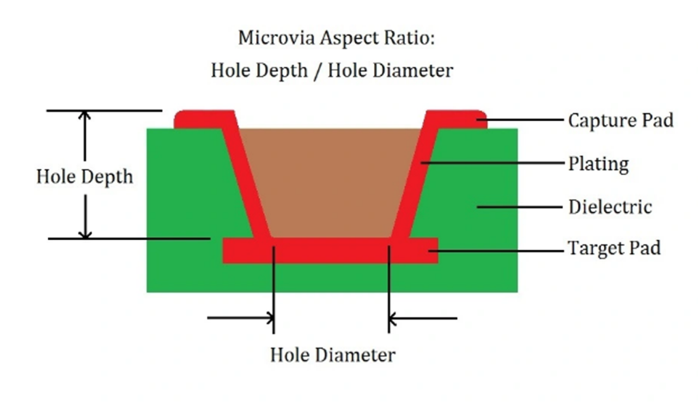
Microvias are widely used in PCB layout and are a key element of high-density design. Without microvias in the small pads of high-density BGAs, processors and memory devices with many pins cannot be routed. Microvias can also be combined with other via types—microvias can be stacked on each other, and can also be stacked with buried or blind vias.
Before managing vias in a design, vias must first be created in the PCB CAD database. You can build via objects yourself or import them from other sources. Most CAD systems provide tools and functions for building vias.
Once vias are built, they can be saved to the company library for use in future designs. In Cadence Allegro X PCB Designer's Constraint Editor, appropriate vias can be assigned to individual nets or net classes for routing.
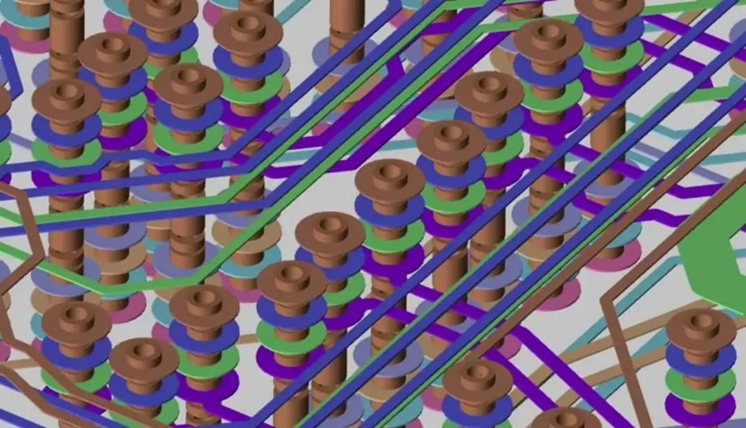
With PCB via design rules, designers can manage the different vias used in a design without manually changing vias for every new net. Once set up correctly, design rules will automatically select the correct via for the net being routed, reducing the designer's workload.
As a factory focused on small-to-medium volume PCB and PCBA manufacturing, AnyPCBA has accumulated years of experience in via processes.
Our manufacturing capabilities cover 2–64 layers, including HDI, rigid-flex, and high-frequency hybrid. We hold ISO 13485 (medical) and IATF 16949 (automotive) certifications.
For via design, our DFM review focuses on:
Whether annular ring dimensions meet reliability class requirements
Whether aspect ratios are within manufacturable limits
Whether via-in-pad designs require microvia or via-fill processes
Whether back drilling requirements have been specified
Whether via tenting or filling methods are clearly defined
Whether blind/buried via stack-ups have been validated
Our engineers help you anticipate via process risks at the design stage, so your boards are not only drawable, but buildable and reliable.
If you're working on via-related PCB design, or want to learn more about our manufacturing capabilities, contact us through our website.
What via design challenges have you encountered? Share your experience in the comments.