
In the rapidly expanding renewable energy sector, the demand for solar inverters that can handle massive current loads without failure has never been higher. A solar inverter is only as reliable as the PCB powering it. If you are struggling with thermal runaway or signal degradation, your choice of PCB manufacturer is likely the culprit. This guide cuts through the noise to help you select a manufacturing partner capable of handling the rigorous demands of high-power energy applications.
Understanding the Role of Heavy Copper in Renewable Energy
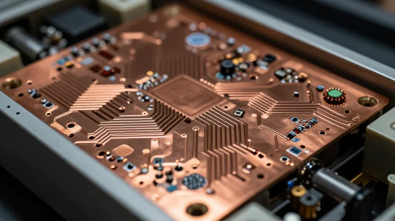
The Engineering Necessity of Heavy Copper
In high-power solar inverter applications, standard PCB designs often fail due to the intense electrical loads and thermal stresses inherent in energy conversion. Heavy copper technology—defined by copper weights exceeding standard 1oz configurations—is the foundational solution for these challenges. By increasing the cross-sectional area of the copper traces, these boards effectively lower electrical resistance, minimizing power losses and preventing catastrophic heat buildup during peak energy generation.
Performance Comparison: Standard vs. Heavy Copper
| Feature | Standard PCB (1oz) | Heavy Copper (3oz-10oz+) |
|---|---|---|
| Current Handling | Low to Moderate | High to Very High |
| Thermal Dissipation | Limited | Excellent heat sinking |
| Mechanical Stress | Prone to delamination | Highly durable |
| Inverter Application | Control/Signal Logic | Power Conversion Stages |
Why Thermal Efficiency Matters for Solar Longevity
Solar inverters must operate reliably for decades, often in harsh, high-temperature outdoor environments. Heavy copper acts as an integrated heat sink, drawing thermal energy away from power components like MOSFETs and IGBTs. This reduction in operating temperature directly translates to longer component life and higher system efficiency, preventing the efficiency derating that occurs when electronics run too hot.
Frequently Asked Questions
- What is the primary benefit of 10oz copper in solar inverters?
The primary benefit is significantly lower resistance, which allows for higher current throughput with minimal voltage drop and heat generation. - Does heavy copper increase the physical size of the PCB?
While the copper thickness increases, it allows for narrower traces to handle the same current, often enabling smaller overall board footprints while maintaining high power density. - Why is thermal dissipation critical for renewable energy projects?
Efficient heat dissipation prevents thermal cycling fatigue, ensuring that the solar inverter remains stable and efficient throughout the duration of its operational lifecycle.
Evaluating Thermal Management Expertise
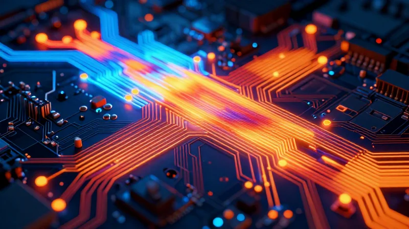
Thermal Management Mastery in Heavy Copper Design
Effective thermal management in heavy copper PCBs requires more than just high-amperage capacity; it demands a synergy between advanced thermal interface materials (TIM), strategic substrate selection, and precise stack-up architecture. When evaluating potential manufacturing partners, assess their ability to integrate high-thermal-conductivity laminates, such as ceramic-filled resins or metal-core alternatives, that prevent localized overheating during sustained peak inverter operation.
Material Selection and Stack-Up Optimization
| Thermal Strategy | Performance Impact | Manufacturer Requirement |
|---|---|---|
| High Tg Laminates | Maintains mechanical stability at extreme temperatures | Must provide Tg data above 170°C |
| Thermal Vias | Facilitates heat transfer to external heatsinks | Copper-filled, capped, and plated via arrays |
| Embedded Heatsinks | Drastically reduces thermal resistance | Advanced milling and press-fit capabilities |
Frequently Asked Questions
- Why is thermal via stitching essential in heavy copper designs?
Thermal vias act as heat conduits from the high-current copper traces to the heatsink; in heavy copper designs, they must be copper-filled to ensure structural integrity and maximum thermal conductivity. - How does stack-up symmetry affect thermal performance?
Symmetrical copper distribution across the PCB stack-up prevents warping during the reflow process, ensuring consistent contact between the PCB and the thermal management system. - Should I prioritize thermal conductivity or dielectric breakdown voltage?
For solar inverters, both are critical; a manufacturer should demonstrate expertise in selecting substrates that balance a high Coefficient of Thermal Expansion (CTE) match with robust dielectric strength to withstand high-voltage surges.
The Necessity of Stringent IPC Quality Standards
Why IPC Compliance is Non-Negotiable
For solar inverters operating in harsh outdoor environments, the PCB serves as the structural and electrical backbone. High-current throughput and significant thermal expansion present risks of delamination, trace cracking, and short circuits. IPC-6012 (Qualification and Performance Specification for Rigid Printed Boards) and IPC-A-600 (Acceptability of Printed Boards) provide the necessary benchmarks for manufacturers to prove their processes can sustain structural integrity under these intense operational stresses.
Critical IPC Benchmarks for Heavy Copper
| Standard | Focus Area | Importance for Solar |
|---|---|---|
| IPC-6012 Class 3 | High-Reliability Boards | Mandatory for mission-critical power electronics. |
| IPC-A-600 | Acceptability Criteria | Visual inspection standards to prevent defect propagation. |
| IPC-TM-650 | Test Methods | Validates thermal stress resistance and copper ductility. |
Addressing Common Compliance Concerns
- Why is IPC Class 3 preferred over Class 2 for solar inverters?
Class 3 standards require stricter hole-fill and plating thickness requirements, which are vital for preventing intermittent connection failures caused by thermal expansion in high-copper-weight boards. - How do IPC standards prevent board delamination?
By enforcing rigorous material testing under IPC-TM-650, manufacturers ensure that the resin-to-copper bond remains intact even when subjected to the rapid thermal cycling typical of solar power conversion. - Can I simply request a 'compliant' board?
No; request specific verification through microsection reports. A reputable manufacturer should provide cross-sectional analysis to prove that plating thickness in the barrel exceeds IPC requirements.
Selecting a manufacturer that operates strictly within IPC guidelines is not just about paperwork; it is an insurance policy for your inverter's field longevity. Manufacturers that prioritize these standards demonstrate a culture of process control, essential when managing the complex plating and etching requirements of heavy copper designs.
Manufacturing Capabilities: Etching and Plating Precision
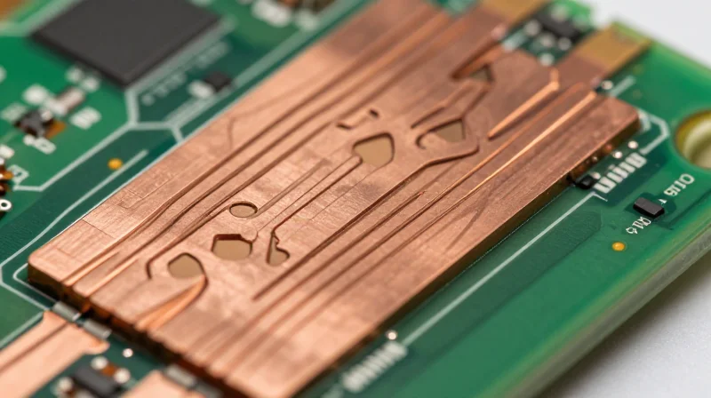
The Challenge of Precision Etching in Heavy Copper
Etching heavy copper (typically 3oz to 10oz+) presents a unique set of manufacturing hurdles, primarily due to the increased etch factor. As copper thickness increases, the chemical etchant takes longer to remove the material, which can lead to significant lateral undercutting of the trace sidewalls. For solar inverter PCBs, this undercutting is catastrophic as it alters trace geometry, resulting in unpredictable impedance, increased parasitic capacitance, and structural weaknesses that fail under mechanical thermal cycling.
Comparing Etching Techniques
| Etching Method | Precision Level | Best Application | Risk |
|---|---|---|---|
| Standard Chemical | Low | Simple Power Planes | High undercut risk |
| Controlled Vertical | High | Inverter Power Stages | Longer processing time |
| Differential Compensation | Very High | Fine-pitch Power/Signal | Complex setup |
Advanced Plating and Uniformity Standards
Plating consistency is equally critical to prevent localized resistance hot-spots. A qualified manufacturer must demonstrate mastery of pulse plating techniques to ensure copper distribution remains uniform across both the hole barrels and the surface features. Without this uniformity, high-current paths experience uneven resistance, leading to thermal gradients that shorten the lifespan of high-power solar inverters.
Manufacturing FAQ
- How does excessive undercut affect my inverter design?
Undercutting reduces the effective cross-sectional area of the trace, increasing DC resistance and causing unexpected heat build-up under high current loads. - What should I look for in a manufacturer's plating process?
Look for pulse plating capabilities, which provide better control over copper deposition in high-aspect-ratio holes compared to traditional DC plating. - Why is trace geometry critical for high-power solar?
Controlled, rectangular trace cross-sections are vital for maintaining predictable impedance and managing mechanical stress induced by extreme temperature fluctuations in outdoor environments.
Supply Chain Stability and Material Traceability
Securing Material Integrity for Solar Reliability
For solar inverter applications, where field deployments often span over two decades, material consistency is non-negotiable. Heavy copper PCBs are subjected to extreme thermal cycling and high current densities, making the selection of high-Tg (glass transition temperature) laminates essential. A reliable manufacturer must guarantee that every batch of substrate and copper foil comes from authorized, tier-one suppliers to prevent performance degradation or premature delamination.
Material Traceability Standards
Implementing a rigorous traceability program allows manufacturers to track every component back to its raw material source. This is vital for root-cause analysis should a failure occur in the field. When evaluating a potential partner, demand proof of supply chain transparency.
| Feature | Standard Requirement | High-Reliability Expectation |
|---|---|---|
| Material Sourcing | Distributor purchase | Direct manufacturer procurement |
| Batch Tracking | Lot number records | Full digital genealogy |
| Material Certification | Generic RoHS compliance | Full COA/COC with thermal testing |
FAQ: Supply Chain and Material Quality
- Why is high-Tg laminate essential for heavy copper PCBs?
High-Tg materials resist deformation at elevated operating temperatures, preventing copper cracking and dielectric failure common in solar environments. - What does full traceability look like?
It is a documented ledger that captures the origin, date of manufacture, and specific testing data for all copper foils, pre-pregs, and solder masks used in your boards. - How do I mitigate supply chain risks?
Avoid low-cost, unverified brokers and prioritize manufacturers who maintain long-term partnerships with established laminate suppliers to ensure component consistency.
Prototyping to Mass Production Scalability
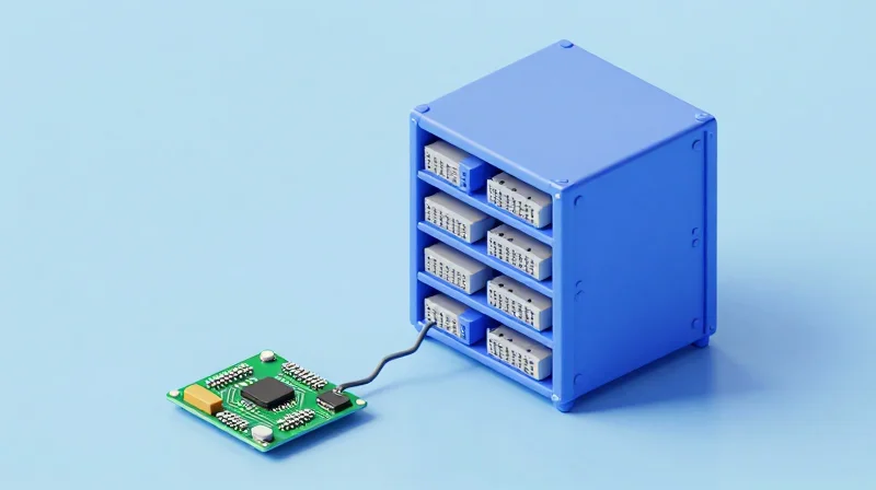
Bridging the Prototyping-to-Volume Gap
Transitioning from a functional prototype to mass production is the most common point of failure for heavy copper projects. Manufacturers often excel at one-off R&D builds but lack the automated infrastructure, standardized process controls, and specialized high-volume etching lines required to maintain the tight tolerances of thick copper layers at scale. Selecting a partner means vetting their capacity to maintain thermal stability and trace integrity across thousands of units without deviating from your initial design specifications.
Prototyping vs. Production Capability Matrix
| Feature | Prototyping Phase | Mass Production Phase |
|---|---|---|
| Process focus | Flexibility & Speed | Efficiency & Repeatability |
| Etching approach | Manual/Semi-automated | Highly automated, controlled spray |
| Quality control | Spot inspection | In-line AOI & flying probe |
| Supply Chain | Ad-hoc purchasing | Strategic material partnerships |
Key Considerations for Scalability
- Does the facility handle volume scaling in-house?
Avoid manufacturers that outsource their production volume to third-party shops, as this breaks the chain of quality control and traceability essential for solar hardware. - How is process repeatability ensured?
Look for manufacturers that use standardized manufacturing execution systems (MES) and automated optical inspection (AOI) capable of detecting under-etched traces in high-copper layers. - What is the engineering support model?
A true partner provides design-for-manufacturing (DFM) feedback during the R&D stage specifically tuned to production-scale limits, such as panel utilization and thermal management optimization.
Ultimately, vetting a manufacturer requires auditing their equipment lifespan and throughput capabilities. Ask for documentation regarding their 'yield-over-time' metrics for heavy copper layers. A manufacturer with a proven track record in high-power energy sectors will have dedicated lines for copper plating that prevent the 'undercut' phenomenon during high-volume etching, ensuring your solar inverters achieve the 20-year operational life expected in the field.
Quality Assurance and Reliability Testing Protocols
In the high-stakes domain of renewable energy, PCB failure in solar inverters can lead to catastrophic system downtime. A qualified manufacturer must demonstrate a comprehensive validation workflow that goes beyond standard electrical continuity checks to address the unique stresses exerted on heavy copper conductors.
Mandatory Validation Protocols for Heavy Copper
| Test Category | Primary Objective | Acceptance Criteria |
|---|---|---|
| Thermal Cycling | Assess copper-to-laminate CTE mismatch | Zero barrel cracking or delamination |
| Cross-Section Analysis | Verify plating thickness and hole structure | Meets IPC-6012 Class 3 requirements |
| High-Voltage Isolation | Ensure dielectric breakdown resilience | Withstand Vrms specified for grid parity |
Structural Integrity and Thermal Reliability
Heavy copper PCBs (typically >3 oz) experience significant localized heating during high-current operations. Cross-sectioning is not optional; it is the only way to inspect the plating uniformity within plated through-holes (PTH). Manufacturers must prove that their plating process prevents 'dog-boning,' which introduces weak points susceptible to thermal fatigue over the solar inverter’s 20-year lifespan.
Frequently Asked Questions on QA Protocols
- Why is thermal cycling critical for solar inverters?
Solar inverters operate in harsh outdoor environments with extreme temperature fluctuations. Thermal cycling tests verify that the heavy copper traces and the substrate expand and contract at rates that do not induce mechanical stress or solder joint fractures. - Does a manufacturer need specialized high-voltage equipment?
Yes. Standard continuity testers cannot detect microscopic dielectric insulation failures. Manufacturers must use automated high-potential (Hi-Pot) testers capable of isolating leakage paths at the high operating voltages typical of modern 1000V+ solar strings. - What should the certificate of conformance (CoC) include?
Beyond basic verification, it should include micro-section photos, TDR reports for impedance control, and ionic contamination test results to ensure that chemical residues from the etching process do not cause long-term electrochemical migration.
Selecting a PCB manufacturer for solar inverters is a long-term strategic investment, not just a procurement task. By prioritizing thermal management, adherence to IPC standards, and manufacturing precision, you safeguard your hardware against field failures. Ready to optimize your power electronics? Contact our engineering team today to discuss your project requirements and ensure your next solar installation is built to last.
