
High-voltage solar systems demand more than just standard circuitry. As power densities climb, traditional PCB fabrication falls short. This guide breaks down the mission-critical DFM protocols required to master heavy copper manufacturing, ensuring your designs survive thermal stress and power spikes without compromising signal integrity.
Understanding the Challenges of Heavy Copper Fabrication
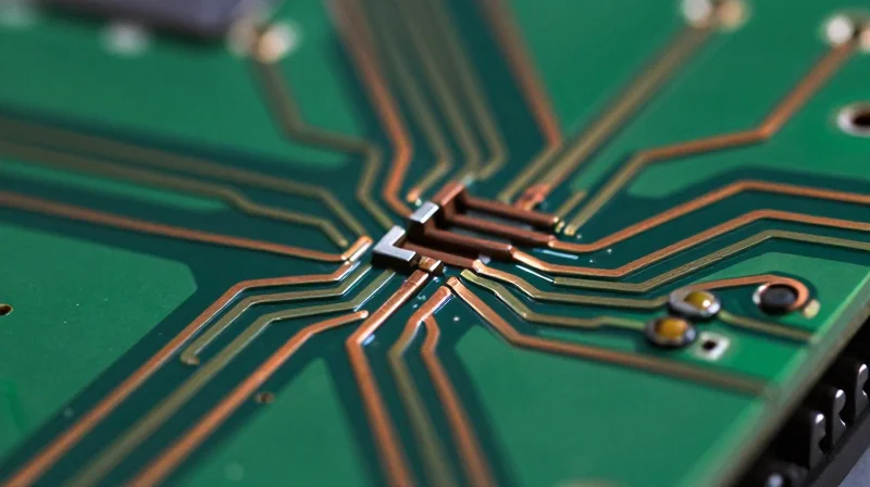
The Etching and Sidewall Geometry Paradox
When copper weight exceeds 3 oz, the primary challenge shifts from standard circuit patterning to structural geometry management. During the chemical etching process, the aggressive dwell time required to remove thick copper can lead to significant 'undercutting' of the trace sidewalls. This lateral etching reduces the copper cross-sectional area, directly impacting the current-carrying capacity calculated during design. Furthermore, as copper thickness increases, maintaining vertical sidewalls—essential for impedance control and insulating spacing—becomes geometrically difficult, often resulting in a trapezoidal profile that must be accounted for in the DFM stackup.
Key Mechanical and Thermal Challenges
| Challenge | Impact | Design Consideration |
|---|---|---|
| Etch Factor | Lateral erosion of trace edges | Increase trace width compensation |
| Thermal Expansion | Stress on plated through-holes (PTH) | Utilize high-Tg, low-CTE materials |
| Surface Planarity | Difficulties in SMT component seating | Employ advanced resin-filling processes |
Frequently Asked Questions on Heavy Copper DFM
- How does copper thickness affect drilling?
Increased thickness requires longer drill dwell times and potentially slower peck cycles to prevent resin smear and copper burring, which can compromise high-voltage dielectric integrity. - Why is board flatness a major concern for heavy copper?
The differential between copper areas and laminate regions causes significant mechanical stress during lamination, which can lead to board warpage and localized delamination. - What role does resin thickness play in voltage breakdown?
With heavy copper, the height of the traces requires significantly thicker prepreg or specialized non-conductive fillers to ensure complete encapsulation, preventing localized electrical discharge or 'corona' effects in solar systems.
Optimizing Etching Processes for Precision and Reliability
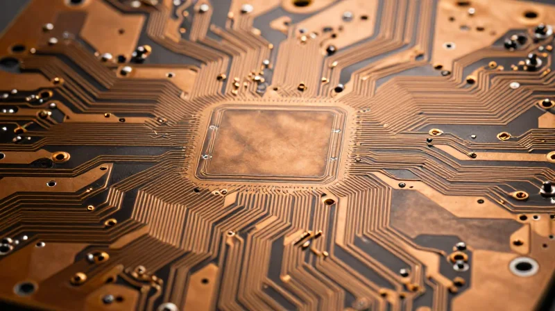
Etching heavy copper (exceeding 3 oz) requires specialized process control because the extended dwell time in the etching solution increases the risk of undercutting, where the etchant attacks the copper laterally beneath the photoresist. To maintain high-voltage isolation, designers must prioritize spacing rules that account for these anisotropic etch characteristics, preventing the formation of copper slivers that lead to catastrophic shorts.
Mitigating Undercut via Design Geometry
The width of the etch factor is directly proportional to copper thickness. As copper weight increases, trace sidewalls become increasingly trapezoidal rather than vertical. Design for Manufacturing (DFM) guidelines mandate compensating for this by widening traces on the artwork and increasing isolation gaps beyond standard tolerances.
| Copper Weight (oz) | Minimum Recommended Gap (mil) | Etch Factor Compensation (mil) |
|---|---|---|
| 3 oz | 15 | 2.5 |
| 4 oz | 20 | 3.5 |
| 6 oz+ | 30+ | 5.0+ |
Preventing Copper Slivers
Copper slivers are small, detached pieces of metal caused by etching isolation gaps that are too narrow for the copper thickness. In high-voltage solar applications, these slivers can act as conductive bridges across creepage distances, resulting in arcing. DFM rules should enforce a strict minimum feature size ratio.
- What is the primary cause of copper slivers?
Slivers occur when the ratio of etching depth to trace spacing results in the collapse of the dielectric material or the isolation gap during the chemical etching process. - How does high voltage change spacing requirements?
In solar systems, you must move beyond standard IPC-2221 spacing to account for potential surge events and dust/moisture contamination that can reduce the effective dielectric strength. - Can solder mask help?
While solder mask is not a substitute for proper etching spacing, using high-voltage rated solder masks can provide a secondary layer of protection against accidental arcing between conductors.
Ultimately, fabricators should utilize pulse-spray etching or specialized chemical additives that enhance etch rate uniformity. Designers must communicate the specific copper weight requirements clearly in the fabrication notes to ensure the etch factor compensation is applied correctly to the specific layer stack-up.
Advanced Plating Techniques for High-Current Vias
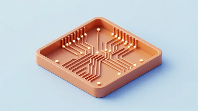
Advanced Plating Techniques for High-Current Vias
Achieving reliable electrical performance in high-voltage solar PCBs requires overcoming the inherent difficulties of plating deep, high-aspect-ratio vias within heavy copper planes. When copper weights exceed 3 oz, standard electrolytic plating often leads to 'dog-boning,' where copper accumulates excessively at the surface entries of the via, leaving the center of the barrel thin or voided. To maintain thermal integrity under continuous high-current loads, fabricators must employ pulse-plating techniques and optimized agitation cycles to ensure consistent, reliable copper distribution across the entire via wall.
Comparative Analysis of Plating Methods
| Method | Effectiveness for Heavy Copper | Primary Advantage |
|---|---|---|
| Standard DC Plating | Low | Simple process control |
| Pulse Plating | High | Superior wall thickness uniformity |
| Conformal Coating/Venting | Medium | Reduced via entrapment |
Plating Best Practices FAQ
- How can I prevent copper voids in high-aspect-ratio vias?
Utilize reverse-pulse plating to improve current density distribution and increase agitation parameters to ensure sufficient electrolyte turnover deep within the hole. - What is the recommended minimum via barrel thickness for 3 oz+ copper?
For high-current solar applications, aim for a minimum of 25 micrometers (1 mil) of copper in the barrel to withstand thermal cycling and high-voltage stress. - Does copper weight influence drill hole size design?
Yes. Larger finished hole diameters are required to compensate for the additional thickness added by the heavy plating process, preventing closure of the via.
Designing Robust Multi-Layer Stackups
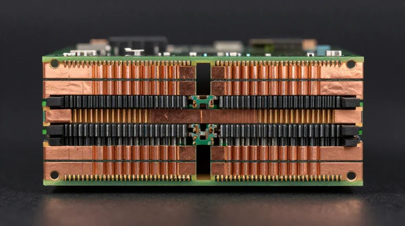
Symmetry and Thermal Stability in Multi-Layer Designs
The primary challenge in multi-layer heavy copper PCB design is mechanical distortion caused by uneven copper distribution. When internal layers feature varying weights or imbalanced copper density, the coefficients of thermal expansion (CTE) mismatch induce stress that leads to bow and twist during lamination or thermal cycling. To mitigate these risks, designers must enforce strict layer symmetry, utilizing identical copper weights on balanced layers relative to the center of the stackup.
Stackup Balancing Comparison
| Design Factor | Imbalanced Design (High Risk) | Balanced Design (Recommended) |
|---|---|---|
| Copper Distribution | Asymmetric weight distribution | Mirror-image layer weights |
| Thermal Dissipation | Localized hot spots/warpage | Uniform heat spreading |
| Structural Integrity | Prone to bow, twist, and delamination | High mechanical stability |
Design Best Practices for High-Voltage Reliability
- How does core material selection impact heavy copper performance?
Use high-Tg (glass transition temperature) laminates with low CTE to ensure the substrate can withstand the mechanical stress of thick copper traces without losing adhesion or suffering barrel cracking. - Why is copper balancing critical for etching?
Balanced copper prevents excessive chemical undercut on one side of the panel compared to the other, which is vital for maintaining the precise line widths required for high-voltage isolation. - What is the recommended pre-preg strategy?
Increase resin content in pre-preg layers between heavy copper planes to ensure complete encapsulation of high-profile traces, preventing air gaps and potential voltage breakdown.
For solar systems requiring long operational lifetimes, consider implementing a 'copper-thieving' strategy—adding non-functional copper patterns—in low-density areas. This process balances the copper-to-dielectric ratio across the entire board surface, further enhancing mechanical uniformity and consistency during the high-temperature press cycle.
Thermal Management and Heat Dissipation Strategies

Heavy Copper as an Integrated Heatsink
In high-voltage solar applications, heavy copper layers—typically 3 oz/ft² or greater—act as primary thermal conductors. To maximize effectiveness, these copper planes must be kept continuous underneath high-heat components. Avoid excessive cutouts or narrow 'neck-down' regions, as these create thermal bottlenecks that increase local junction temperatures, potentially leading to premature dielectric degradation.
Thermal Via Strategy and Stitching
Thermal vias serve as the critical bridge between component thermal pads and internal heavy copper layers. For high-current density, prioritize large-diameter, copper-plugged, and capped vias to ensure a high-conductivity path while preventing solder wicking during assembly.
| Via Type | Thermal Performance | Dfm Complexity | Best Application |
|---|---|---|---|
| Through-hole (Open) | Low/Moderate | Low | Low-current general cooling |
| Via-in-Pad (Capped) | High | High | High-power MOSFETs/IGBTs |
| Copper Filled/Plated | Maximum | Very High | Critical high-voltage nodes |
Thermal Relief Design Principles
In heavy copper designs, standard thermal relief spokes are often insufficient and may act as current limiters that heat up under high-load conditions. Use 'Direct Connect' or solid copper fills whenever assembly manufacturing processes allow, utilizing high-temperature solder profiles to mitigate the risk of cold solder joints.
FAQ: Managing Heat in Solar PCBS
- Why avoid standard narrow spokes in heavy copper?
Narrow spokes create high-resistance paths that act as fuses; in solar systems, these become localized hotspots that reduce long-term reliability. - How does board thickness affect thermal dissipation?
Thicker boards with heavy copper increase the overall thermal mass, which slows down temperature rise but necessitates higher energy input during reflow to ensure proper wetting. - What is the best way to handle thermal expansion?
Use balanced copper distribution on both sides of the PCB to prevent warping, and select high-Tg (glass transition temperature) laminate materials to withstand operating temperatures exceeding 130°C.
Surface Finish Selection for Extreme Power Environments
In heavy copper applications, the surface finish must do more than protect against oxidation; it must withstand extreme thermal cycling and support massive current loads without becoming a point of electrical resistance. While standard finishes suffice for signal integrity in low-power boards, high-voltage solar modules require finishes that maintain mechanical integrity and prevent diffusion-related failures at the intermetallic interface.
Comparative Analysis of Surface Finishes
| Finish | Thermal Reliability | Current Carrying Impact | Best Use Case |
|---|---|---|---|
| ENIG | Excellent | Moderate (Nickel Barrier) | High-reliability control circuitry |
| HASL (Lead-Free) | Good | Superior (High Solder Volume) | High-current power connections |
| Immersion Silver | Moderate | Excellent (Low Resistance) | Complex layouts needing flatness |
Critical Performance Considerations
For heavy copper systems, the primary concern is the nickel-phosphorus layer inherent in Electroless Nickel Immersion Gold (ENIG). While ENIG offers excellent planar surfaces, the nickel layer can introduce significant impedance at very high current densities. Conversely, Lead-Free Hot Air Solder Leveling (HASL) provides a robust, thick layer of solder that reinforces connections, making it highly desirable for high-vibration, high-current environments common in solar installations.
Frequently Asked Questions
- Does ENIG affect the conductivity of heavy copper traces?
Yes, the nickel layer has significantly higher electrical resistance than copper. For paths carrying hundreds of amperes, minimize ENIG use in the direct power path to prevent localized heating. - Why is HASL often preferred for high-current solar applications?
HASL provides a thicker intermetallic bond and superior solder volume, which enhances the mechanical fatigue resistance needed for boards subjected to daily thermal expansion and contraction cycles. - Is Immersion Silver recommended for long-term outdoor solar exposure?
No, Immersion Silver is prone to tarnishing and potential creep corrosion. It is generally not recommended for high-voltage solar systems exposed to high humidity and temperature fluctuations unless the enclosure is hermetically sealed.
DFM Verification: Preventing Common Manufacturing Pitfalls
Critical Pre-Production Design Verification
Before transitioning to production, heavy copper designs must undergo rigorous DFM verification to address the unique mechanical and electrical constraints inherent in high-current solar applications. Failure to validate these parameters often leads to inner-layer registration issues, insufficient etch factors, and catastrophic failure under high-voltage arcs.
Common Manufacturing Pitfalls Checklist
- Undercutting and Etch Compensation
Heavy copper traces experience significant lateral etching. Ensure your CAD tool accounts for trace width reduction to hit final target impedance and current capacity. - Aspect Ratio and Plating Voids
High-current boards often use thicker cores. Verify that your hole diameter-to-depth ratio remains within the fabricator's capability to ensure uniform barrel plating. - Solder Mask Dam DFM
Avoid 'mask bleed' by ensuring sufficient clearance between high-voltage pads and copper pours to prevent unwanted bridges during reflow. - Clearance and Creepage
Maintain rigorous physical spacing between high-voltage nodes to prevent tracking and arcing, especially in dusty solar environments.
DFM Verification Matrix
| Parameter | Typical Issue | DFM Mitigation Strategy |
|---|---|---|
| Copper Weight | Warpage/Twist | Symmetric layering/stackup |
| Trace Spacing | Etching/Shorts | Increase gap width (min 10-15 mil) |
| Via Placement | Plating Voids | Avoid excessive via clustering |
| Edge Clearance | Mechanical Stress | Respect 20-mil board edge keep-out |
To expedite turnaround, perform a 'DFM handoff' meeting with your fabricator specifically reviewing the heavy copper etch compensation requirements. This communication loop typically catches design bottlenecks that automated DFM checkers might overlook.
The Role of Collaboration with Fabrication Partners
The Strategic Necessity of Early Design Engagement
In the context of high-voltage solar systems, heavy copper PCBs (typically 3oz to 10oz+) present unique fabrication challenges that go beyond standard signal-level board production. Engaging with your fabrication partner during the schematic and layout phase is the single most effective way to avoid costly re-spins. Manufacturers can provide critical insights into etching tolerances, plating thickness uniformity, and thermal expansion properties that are specific to their equipment, ultimately preventing field failures in harsh solar environments.
Key Areas for Manufacturer Consultation
| Design Factor | Manufacturer Influence | Risk if Ignored |
|---|---|---|
| Copper Thickness | Determines etch factor and trace spacing | Short circuits or insufficient current capacity |
| Prepreg Selection | Controls dielectric breakdown/HV clearance | Dielectric failure under high-voltage load |
| Via Structure | Advises on optimal hole-wall copper plating | Via cracking during thermal cycling |
Common Collaboration Queries
- When is the optimal time to involve the manufacturer?
Ideally, engage during the preliminary layout phase. Establishing copper weight requirements and stack-up constraints before final routing ensures that trace widths and air gaps comply with DFM standards. - How does collaboration reduce lead times?
By aligning design parameters with the manufacturer's internal process capabilities (such as standard panel utilization), you eliminate 'query loops' where a design is paused to resolve manufacturability concerns. - Can the fabricator help with thermal reliability?
Yes, many manufacturers offer DFM analysis tools that simulate the thermal expansion behavior of heavy copper, allowing them to suggest optimized via arrays that prevent delamination.
Ultimately, the partnership between the design engineer and the fabrication house is a bridge between theoretical performance and physical reality. Treating the manufacturer as an extension of your design team ensures that your heavy copper solar boards are optimized for both high-voltage endurance and manufacturability, securing the longevity of the entire solar energy system.
By adhering to these rigorous DFM standards, you can transform high-voltage board challenges into competitive performance advantages. Don't let manufacturing constraints hinder your innovation. Contact our engineering team today to review your current heavy copper stackup and ensure your next solar project is built for maximum reliability.
