From the intricate circuitry of our smartphones to the robust control systems of industrial machinery, Printed Circuit Boards (PCBs) are the unsung heroes of modern electronics. But what exactly determines the cost of these essential components? This article breaks down the complex factors contributing to PCB costs and offers clear, actionable strategies to manage and minimize your expenses. Understanding these nuances is critical for projects large and small, ensuring your designs remain both innovative and affordable, balancing advanced tech with careful consideration of pcb cost.
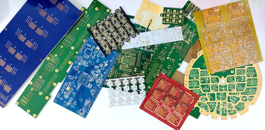
Understanding the key factors that influence Printed Circuit Board (PCB) cost is crucial for effective design and budget management. These factors range from fundamental material choices and design complexities to manufacturing processes and assembly requirements. This section provides a foundational overview of the primary cost drivers associated with PCB fabrication, setting the stage for subsequent, more detailed analyses.
Several interconnected elements contribute to the overall PCB cost. These include:
Each of these factors, and their interplay, contributes to the total cost of PCB production. A strategic approach to PCB design and manufacturing requires a comprehensive understanding of these cost drivers.
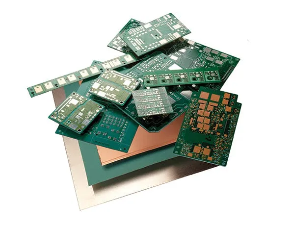
The selection of dielectric materials is a critical factor influencing both the performance and cost of a printed circuit board (PCB). Different materials offer varying electrical, thermal, and mechanical properties, which directly affect the manufacturing process and the final cost. Understanding these trade-offs is essential for optimizing PCB design for specific applications while controlling expenses.
| Material | Description | Relative Cost | Typical Applications |
|---|---|---|---|
| FR-4 | The most common PCB material, composed of woven fiberglass cloth with epoxy resin. Offers good electrical insulation, mechanical strength, and is relatively low-cost. | Low | Most standard electronic applications, general purpose boards. |
| Aluminum | Aluminum substrates offer excellent thermal conductivity and are typically used where heat dissipation is critical, such as in LED lighting and power electronics. | Moderate to High | LED lighting, power converters, high-power electronics |
| Polyimide | High-performance material with superior high-temperature stability and chemical resistance. Used in flexible circuits, high reliability, and high temperature environments. | High | Aerospace, automotive, medical, flexible electronics |
| Rogers Materials | Specialized materials with very low signal loss and stable electrical properties, suitable for high-frequency applications. | High | RF and microwave applications, high-speed digital circuits. |
| CEM-1/CEM-3 | Alternative to FR-4 with good performance for consumer electronics and cost-sensitive applications. CEM-3 has better mechanical strength than CEM-1 | Low to Moderate | Consumer electronics, simple electronic devices |
In conclusion, the selection of PCB materials is a balancing act between cost and performance requirements. The choice should align with the specific needs of the project, considering factors such as thermal management, electrical performance, and environmental conditions. By carefully analyzing these aspects, engineers can design cost-effective PCBs without compromising the functionality and reliability of the final product.
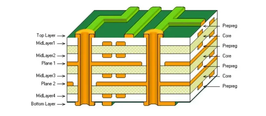
The number of layers in a printed circuit board (PCB) is a fundamental determinant of its cost and complexity. Ranging from simple single-layer boards to intricate multi-layer designs, each layer adds to the manufacturing process, directly affecting the final price. Understanding this relationship is crucial for cost-effective PCB design.
The number of layers directly impacts manufacturing processes, materials usage, and fabrication complexity, as the fabrication process is increasingly complex with each layer added to the board, consequently raising production costs.
| PCB Layer Type | Complexity | Typical Applications | Cost Implication |
|---|---|---|---|
| Single-Layer | Simplest design with all components and traces on one side. | Basic electronics, simple circuits, educational boards. | Lowest cost, easiest to manufacture. |
| Double-Layer | Traces on both sides; allows for more complex routing. | Consumer electronics, simple controllers, basic test equipment. | Moderate cost, increased complexity |
| Multi-Layer | Three or more layers; allows for highly complex and dense routing. | Advanced electronics, high-speed digital systems, complex devices. | Highest cost, most complex to manufacture. |
Here is a breakdown of the primary cost drivers related to the number of PCB layers:
Strategic layer selection is a key aspect of cost optimization. Consider these points when determining the number of layers:
By carefully analyzing the application requirements and weighing the cost implications, engineers can make informed decisions about the number of PCB layers required, ultimately minimizing the overall PCB cost.
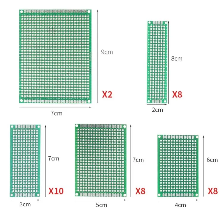
The physical dimensions and shape of a Printed Circuit Board (PCB) significantly affect its overall cost. Larger boards consume more raw material, while complex outlines with numerous cutouts increase manufacturing time and material waste, directly impacting the final price.
Understanding how board size and shape influence PCB cost is crucial for optimizing designs. By carefully considering these factors, designers can minimize waste and reduce overall expenditure without compromising functionality.
| Factor | Impact on PCB Cost | Cost Reduction Strategy |
|---|---|---|
| Board Size | Larger boards increase material consumption and processing time, raising costs. | Minimize board area to the necessary size for components and functionality. |
| Board Shape Complexity | Complex shapes and numerous cutouts lead to increased material waste and longer manufacturing times. | Simplify board outlines where possible; reduce the number and complexity of cutouts. |
| Panel Utilization | Inefficient use of panel space leads to material wastage. | Optimize board layout to maximize panel utilization. |
To further illustrate, let's consider the impact of board shape on costs. Rectangular or square boards are the most cost-effective to manufacture due to efficient material usage. However, if a design necessitates a unique shape, for example, a circular or an 'L' shaped PCB, costs will rise due to the increased complexity and material wastage from the cutouts. This waste material is known as 'scrap' and is generally factored into the overall cost per board.
In essence, a seemingly simple change in PCB outline may have a significant impact on the total cost. Careful planning and design decisions that consider the manufacturing process can help avoid unnecessary expense. Additionally, consult with manufacturers regarding optimized panelization strategies; aligning the board shape and layout with panelization can significantly improve material utilization and lower cost per unit.
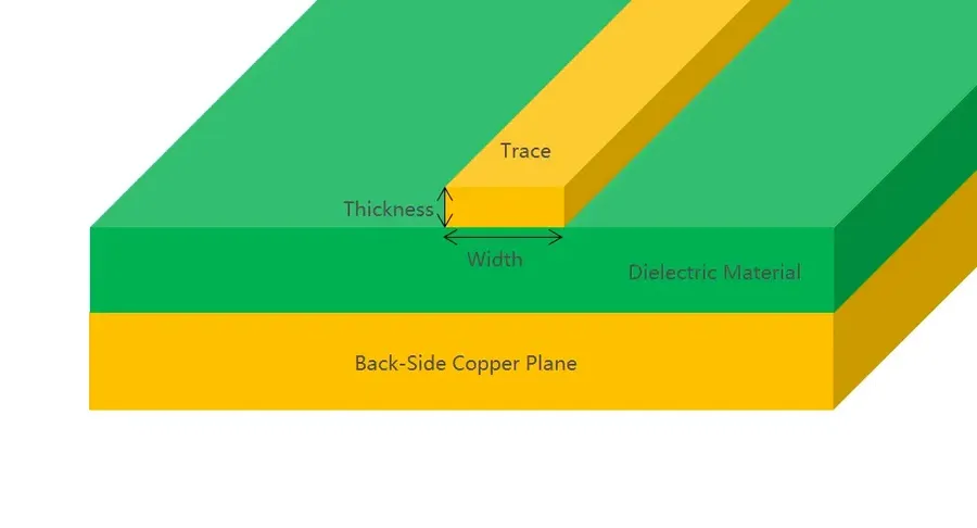
The precision demanded by trace width, spacing, and vias directly influences PCB manufacturing cost. Finer features and higher densities necessitate advanced manufacturing techniques, which translate to higher fabrication costs. This section delves into the relationship between design choices and their cost implications.
Achieving the desired electrical performance often involves specifying precise trace widths and spacing. This impacts not only functionality but also cost, as tighter tolerances require more advanced and controlled manufacturing processes.
| Feature | Impact on Cost | Reason |
|---|---|---|
| Narrower Trace Width | Higher | Requires higher resolution photolithography and more precise etching. |
| Smaller Trace Spacing | Higher | Increases density and requires advanced imaging techniques. Higher risk of shorts during manufacturing. |
| Smaller Vias | Higher | Demands high-precision drilling and plating processes. Microvias increase costs significantly. |
| High-Density Layout | Higher | Complex design rules require sophisticated equipment and rigorous quality control, adding to the cost. |
When designing for cost-effectiveness, consider the following guidance:
The cost implications of trace widths, spacing, and vias should be weighed against the functional requirements. While optimizing for cost is important, it is critical to maintain signal integrity and performance.
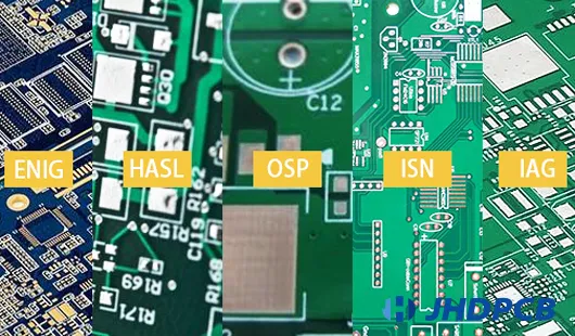
The surface finish of a PCB is a critical factor that impacts both its performance and manufacturing cost. Selecting the right finish is essential for ensuring reliable solderability, corrosion resistance, and overall functionality, while also balancing budgetary constraints. The choice directly influences the long-term reliability and cost-effectiveness of the final product.
| Surface Finish | Description | Cost | Pros | Cons | Typical Applications |
|---|---|---|---|---|---|
| HASL (Hot Air Solder Leveling) | Molten solder is applied to the board, and excess solder is removed by hot air knives, leaving a thin coating. | Low | Good solderability, low cost, widely available. | Uneven surface, not suitable for fine pitch components, leaded option has environmental concerns. | General purpose boards, prototyping, through-hole components |
| Lead-Free HASL | Similar to HASL but uses a lead-free solder alloy. | Low to Mid | Good solderability, compliant with RoHS, widely available. | Uneven surface, not ideal for very fine pitch. | General purpose boards, compliant with environmental standards |
| ENIG (Electroless Nickel Immersion Gold) | A layer of nickel is plated onto the copper, followed by a thin layer of gold. | High | Excellent solderability, good for fine pitch components, good shelf life. | High cost, 'Black Pad' issue can be a concern with certain process controls. | Fine-pitch components, wire bonding, demanding applications |
| Immersion Tin | A thin layer of tin is chemically deposited onto the copper surface. | Mid | Good solderability, flat surface, lead-free. | Can be prone to whisker growth, shorter shelf life compared to ENIG. | Lead-free applications, mid-range cost |
| Immersion Silver | A thin layer of silver is chemically deposited onto the copper surface. | Mid | Good solderability, flat surface, lead-free. | Susceptible to tarnishing, can have a shorter shelf life if not handled properly. | Lead-free applications, mid-range cost |
| OSP (Organic Solderability Preservative) | A thin organic coating is applied to protect the copper from oxidation. | Low | Good solderability, low cost, flat surface. | Short shelf life, sensitive to handling, requires fluxing for soldering. | General purpose boards, cost-sensitive applications, wave soldering. |
The choice of surface finish is a trade-off between cost, performance, and application requirements. For instance, while HASL is the least expensive, it is not suitable for boards with fine-pitch components, making ENIG a better option despite the higher cost. Similarly, while OSP offers a low cost, its limited shelf life and sensitivity to handling are significant drawbacks that may make it less ideal for certain manufacturing environments. It is important to consider these trade-offs in your design to optimize both cost and performance.
Key considerations when selecting a PCB surface finish include the types of components to be soldered, the operating environment of the final product, required board shelf life, and of course, the cost. A thorough analysis of these factors in the design phase ensures that the selected finish aligns with both functional and economic goals, leading to a more reliable and cost-effective final product.
The chosen manufacturing process significantly influences the unit price of Printed Circuit Boards (PCBs). Understanding how different production techniques impact cost is crucial for selecting the most appropriate strategy for varied project scales, directly affecting the overall PCB cost.
| Process Type | Volume | Cost per Unit | Lead Time | Typical Use Cases |
|---|---|---|---|---|
| Prototyping | Very Low (1-10 boards) | High | Fastest | Initial design verification, rapid iteration. |
| Small Batch Production | Low (10-100 boards) | Medium to High | Medium | Early product development, pilot runs. |
| Medium Volume Production | Medium (100-1000 boards) | Medium | Medium | Trial runs, small scale market deployment. |
| High Volume Production | Large (1000+ boards) | Low | Longest | Mass production, established products. |
The above table illustrates a general trend; specific pricing will vary depending on complexity and manufacturer. Prototyping involves high per-unit cost because of set-up overheads associated with each design iteration, like setting up machines for a small number of boards. In contrast, mass production amortizes these costs across a larger batch, significantly lowering individual unit costs. The lead time is another crucial factor, with prototyping demanding faster delivery, while high volume production can be planned in advance.
Furthermore, choosing between local and overseas manufacturers impacts lead time and cost. Domestic providers often offer faster turnaround but may come with higher production costs. Conversely, overseas manufacturers may provide cheaper options, but with increased lead times and communication hurdles.
In conclusion, aligning the production volume and method with the project phase is critical for cost optimization. Prototyping is designed for design validation, small batches for early development, and large scale production for market ready products. Understanding the economic trade offs involved in these various techniques is crucial to manage PCB related costs.
PCB assembly costs are a significant portion of the total expense when producing electronic devices. These costs are influenced by a range of factors, from the complexity of the design and the components used to the manufacturing process itself. Understanding these elements is crucial for effective cost management.
PCB assembly involves populating a bare printed circuit board with electronic components. This process generally includes several steps: solder paste application, component placement, soldering (reflow or wave), inspection, and potentially testing. Each of these steps contributes to the final assembly cost.
| Cost Factor | Description | Cost Impact |
|---|---|---|
| Component Costs | Price of individual electronic parts | High, often the largest contributor |
| Placement Complexity | Number of parts, package type and placement density | Moderate to High, increased complexity leads to increased cost. |
| Soldering Methods | Reflow, Wave, Selective Soldering | Moderate, depends on the method and equipment. |
| Inspection and Testing | Automated, X-ray, functional test | Moderate, increases with testing rigour |
| Lot Size | Number of boards in a production run | Significant, inversely related to per-unit cost. |
Understanding the various factors influencing PCB cost is crucial for effective budget management in electronics projects. This section addresses common questions about PCB costs, providing clear and concise answers to guide your decision-making.
Understanding the nuances of PCB cost is essential for any project involving electronics. By considering material choices, design complexity, and manufacturing processes, you can make informed decisions that not only meet your functional requirements but also manage your budget effectively. Whether you're seeking a cost-effective prototype or a large-scale production run, these strategies will help you navigate the complex landscape of pcb cost, ensuring you receive the best value without sacrificing quality. Optimizing pcb cost requires a comprehensive view of design and manufacturing, allowing you to make the best choices for your specific situation. Remember that early consideration of these elements can lead to significant cost savings without compromising performance.

