
AnyPCBA PCB and PCBA case studies


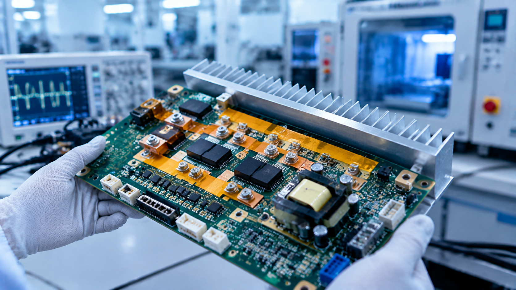
Introduction: A real-world case study of a high-voltage electrosurgical generator PCBA: 4000Vpp output, 460kHz, 300W+, targeting zero field failures within 12 months. This case covers high-voltage isolation, creepage distance control, SiC-based thermal management, EMI suppression, and reliability verification for medical-grade PCBA manufacturing.
Description: Based on AnyPCBA's high-reliability medical PCBA manufacturing experience, this case study explains how high-voltage isolation, thermal balance, EMI suppression, and manufacturing process control achieved zero field failures in an electrosurgical generator PCBA.
In early 2025, a Chinese medical device company specializing in minimally invasive surgical equipment approached us. Their next-generation electrosurgical generator needed to meet a demanding set of requirements.
Customer requirements and pain points:
High-voltage output: maximum output voltage ≥4000Vpp, frequency 460kHz, power ≥300W, supporting pure cut, coagulation, and blend modes
Reliability target: field failure rate (FFR) ≤0 ppm within 12 months of market launch (zero field failures)
Compliance requirements: GB 9706.1 (medical electrical equipment safety), GB 9706.4 (high-frequency surgical equipment safety), IEC 60601-1-2 (EMC), and NMPA Class II medical device registration
Environmental adaptability: stable operation in typical operating room temperature and humidity (20–30°C, 40%–70% RH) and electromagnetic interference (from electrosurgical pencils, anesthesia machines, etc.)
Core challenges: the "three difficulties" of high-voltage PCBA
High-voltage isolation and creepage distance: 4000Vpp requires ≥8mm creepage distance on the PCBA (mandatory per GB 9706.4), while avoiding surface discharge or breakdown caused by moisture and dust
Power loss and thermal management: a 300W-class power amplifier circuit generates significant heat in a confined space. Excessive temperature rise reduces component life and can even cause insulation failure
EMI suppression: high-frequency, high-voltage circuits generate electromagnetic radiation that can interfere with the device's own control circuits (MCU, sensors) and other medical equipment. Must meet YY 0505 Class B limits
Zoning isolation and creepage distance control: the PCBA was divided into a high-voltage zone (power amplification, high-voltage output), a low-voltage zone (control, communication), and an isolation buffer zone. A ≥10mm physical isolation band (no traces, no pads) was placed between high-voltage and low-voltage zones. Critical high-voltage trace spacing was ≥8mm (10mm in actual design), with copper pour and grounding on both sides of the traces to form a "shielding wall."
Insulation material upgrade: the high-voltage zone uses high-CTI FR-4 (CTI≥600V). Insulating gaskets and silicone rubber encapsulation (thickness ≥1.5mm) are used between pads to prevent tracking under humid conditions.
Redundant protection circuits: dual overvoltage/overcurrent protection is designed—hardware uses TVS diodes + gas discharge tubes (GDT), and software uses the MCU to monitor output voltage/current in real time, cutting off high-voltage output within 0.1ms during anomalies to prevent fault escalation.
Low-loss power device selection: SiC MOSFETs replaced traditional silicon MOSFETs, reducing on-resistance by 60% and switching losses by 40%, with heat generation reduced by 35% at the same power level.
High-efficiency thermal design: a large copper area plus a thermal via array (0.3mm diameter, 1.2mm pitch) beneath power devices (SiC MOSFETs, transformers) conducts heat to an aluminum heatsink on the PCB backside. High-thermal-conductivity silicone (≥3W/m·K) fills the gap between heatsink and enclosure, forming a "chip → PCB → heatsink → enclosure" thermal path.
Thermal simulation verification: ANSYS Icepak simulation optimized heatsink fin spacing and fan speed (if needed), ensuring power device junction temperature ≤85°C (below the 105°C rated maximum) at full power, with overall PCBA temperature rise ≤15°C (meeting GB 9706.1 limits).
High-frequency circuit layout optimization: the high-voltage power amplifier uses "star grounding" to avoid ground loop current interference. High-frequency signal traces (such as drive signals) are kept ≤50mm, with ground pour on both sides to reduce antenna effects.
Filtering and shielding: a π-type filter circuit (common-mode inductor + X/Y capacitors) is added between the high-voltage output and low-voltage control ends to suppress conducted interference. The entire PCBA is coated with conductive carbon powder (surface resistivity ≤10Ω/sq) and bonded 360° to the metal enclosure, forming a full shield.
EMC pre-testing and correction: radiated and conducted disturbance pre-tests are performed in an anechoic chamber. For frequencies exceeding limits (such as the 460kHz fundamental and its harmonics), magnetic rings, drive resistor adjustments, or PCB stack-up optimization are applied to ensure margin ≥6dBμV/m.
High-voltage soldering process: high-voltage zone pads use large pads with thick solder paste (0.15mm stencil) to ensure full solder fill and reduce localized heating from cold joints. After soldering, 100% X-ray inspection (AXI) is performed to check for internal voids (void rate <3%).
Cleanliness control: production environment is ISO Class 7 (10,000-class) cleanroom. PCBA cleaning uses "deionized water + IPA ultrasonic cleaning" to remove flux residue (ionic contamination <1.56μg/cm², meeting IPC-J-STD-001).
Reliability stress testing: high-temperature aging (85°C/1000h), thermal cycling (-40°C to 85°C, 500 cycles), and damp heat testing (40°C/93% RH, 1000h) verify high-voltage insulation performance (insulation resistance ≥100MΩ) and functional stability, ensuring no breakdown and no parameter drift.
This case is one of the typical experiences AnyPCBA has accumulated in high-reliability medical PCBA manufacturing. Our role is not just to build to the drawing—we step in at the DFM review stage to help customers identify manufacturing risks related to high voltage, thermal management, and EMI.
In this project, AnyPCBA was involved in:
High-voltage zone creepage distance and isolation band review: confirming the manufacturability of the 10mm physical isolation band and 10mm high-voltage trace spacing
Insulation material process support: evaluating the processing window for high-CTI FR-4 and the feasibility of insulating gaskets + silicone rubber encapsulation
Thermal via array process confirmation: drilling precision and hole wall quality for 0.3mm diameter, 1.2mm pitch thermal via arrays
Thick solder paste printing process: printing window and paste fill consistency for 0.15mm stencils
100% X-ray inspection: void rate detection for high-voltage zone solder joints, ensuring <3%
Cleanroom production and cleaning process: ISO Class 7 cleanroom environment, deionized water + IPA ultrasonic cleaning, ionic contamination <1.56μg/cm²
Reliability stress testing support: working with the customer to complete high-temperature aging, thermal cycling, and damp heat testing
Our manufacturing capabilities cover 2 to 64 layers, including HDI, rigid-flex, and high-frequency hybrid. We hold ISO 13485 (medical) and IATF 16949 (automotive) certifications, with extensive experience in medical electronics, industrial power, and automotive electronics.
If you're working on a high-voltage PCBA or high-reliability medical electronics project, contact us through our website. Our engineers can help you anticipate these "physical-path-determined" performance risks at the design stage.


