Introduction: AI is starting to enter EDA tools and take on real PCB design tasks. This article explores what AI can and cannot replace, why engineering judgment still matters, and how the role of PCB engineers is being redefined.
Description: Based on AnyPCBA's small-to-medium volume PCB manufacturing experience, this article explains how AI is reshaping PCB design workflows—and why the ability to judge manufacturability, define constraints, and control risk will become the real competitive advantage for engineers.
Recently, as large language models have become more capable, some people have even demonstrated letting AI directly operate KiCad to complete PCB design tasks. Many PCB engineers are starting to worry: will AI eventually replace PCB engineers too?
Our take:
PCB engineers will not be replaced wholesale by AI, but the role will definitely be redefined by AI. And the part of the job that is purely "operating software and drawing the board" will be hit first.
In the past, AI mostly answered questions: How should high-speed traces be routed? How should differential pairs be handled? What should power layout pay attention to?
Now it's different. AI has started entering EDA tools and directly executing design tasks.
This means many rule-based, highly repetitive tasks may gradually be handed over to AI. For example: basic placement and routing, repetitive modifications, rule checks, documentation organization, and version adjustments.
These tasks are essentially "execution." As long as the rules are clear enough, AI will get better and better at them.
So if a PCB engineer's core competitiveness is only:
Being very proficient in Altium Designer
Being very proficient in PADS
Being very proficient in Allegro
Someone gives me a schematic, and I draw the board
Then yes, there is reason to feel a sense of urgency.
The hardest part of a real project is never how to operate the software. Often, even "what the rules should be" requires the engineer to judge for themselves.
Real projects usually look like this:
The mechanical structure is already fixed
Cost cannot increase
Space is tight
Lead time is urgent
EMC must still be passed
Performance, manufacturability, and reliability conflict with each other
At this point, the valuable question is not "how should this trace be routed?" but rather: how should this board actually be designed?
You have to judge: What matters most? Where is the highest risk? What must be insisted on? What can be compromised? Why must this component go here? Why can't this trace be routed that way? If the board comes back with a problem, where do you start locating it?
These abilities are not gained simply by being proficient with EDA tools. They require: engineering judgment.
Layer 1: Standardized work handed to AI.
Basic placement, partial routing, checks, modifications, and documentation will increasingly involve AI.
Layer 2: AI designs first, engineers review and optimize.
Engineers may not personally draw every trace, but they must know why the critical traces are routed the way they are.
Layer 3: For complex projects, engineers define constraints and make technical decisions.
AI can find solutions based on rules. But first, someone has to tell it: what exactly are the rules?
This is the real value of a high-level PCB engineer.
In the past, a project might require several people to complete. In the future, one experienced engineer working with AI may be able to accomplish the workload of several people.
So the demands companies place on PCB engineers will not decrease—they will increase.
What companies are truly willing to pay for is no longer just: "You draw boards fast." It's: "I trust you with this board."
You can understand the product. You can define constraints. You can judge risks in advance. You can spot problems in AI's proposals. And when the board comes back with issues, you can still trace and solve them.
This is the real value of an engineer.
As a factory focused on small-to-medium volume PCB and PCBA manufacturing, AnyPCBA has observed something interesting as AI design tools become more widespread:
AI makes design faster, but the communication cost from design to manufacturing has not decreased—in some cases, it has actually increased.
The reason is simple: AI-generated solutions are often "correct" in terms of electrical rules, but not necessarily "manufacturable" in terms of process.
For example:
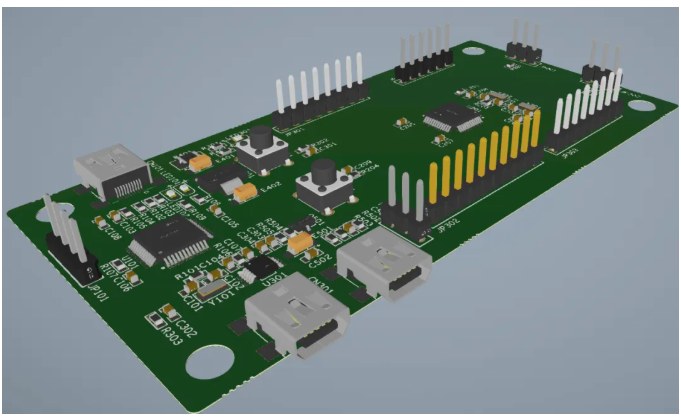
AI may place vias on pads, which can cause solder wicking under certain processes
AI may choose the finest line width to meet routing density, ignoring the factory's minimum line width capability
AI may generate an asymmetrical stack-up without considering warpage risk during lamination
AI may overlook panelization design, leading to stress concentration during depanelization
AI won't proactively tell you about these issues. But engineers on the manufacturing side will catch them during DFM review.
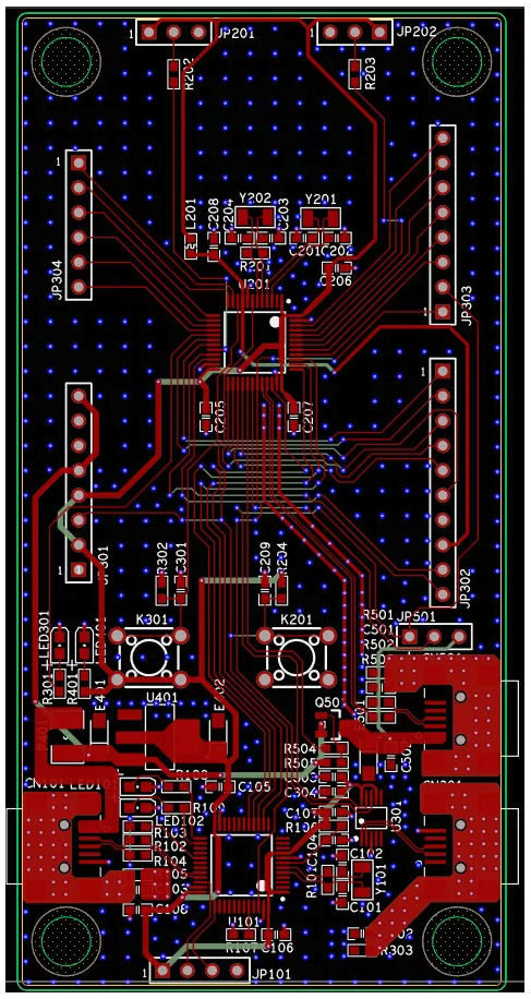
So we believe that the core competitiveness of future PCB engineers is not just being able to use AI to draw boards, but being able to judge whether the boards AI draws can be manufactured and reliably mass-produced.
AI will not make PCB engineers unemployed, but it will make engineers who only know how to draw boards unemployed.
Future PCB engineers need to shift from "executors" to "decision-makers"—understanding the product, defining constraints, judging risks, and controlling manufacturability.
AnyPCBA has over ten years of experience in small-to-medium volume PCB manufacturing, specializing in 5–5000 pcs production with no MOQ for prototype boards. Our manufacturing capabilities cover 2–64 layers, including HDI, rigid-flex, and high-frequency hybrid. We hold ISO 13485 (medical) and IATF 16949 (automotive) certifications.
As AI design tools become more widespread, AnyPCBA's engineers focus on stack-up design, impedance control, minimum line width/spacing, via processes, panelization methods, and special process feasibility during DFM review—helping you anticipate manufacturing risks at the design stage. We aim to be an effective bridge between design and manufacturing, so your boards are not only drawable, but buildable and reliable.
If you're working on PCB design, or looking for a manufacturing partner who understands design intent and helps you anticipate risks during DFM, contact us through our website.