
In the high-stakes world of robotics, the difference between a seamless motion sequence and a catastrophic system failure often lies in the sub-millimeter details of your PCB. As component density increases and form factors shrink, engineers must move beyond basic design practices to adopt rigorous Design for Manufacturing (DFM) protocols. This guide outlines the essential technical framework required to ensure your mission-critical hardware meets the highest standards of reliability, signal integrity, and thermal efficiency.
The Imperative of Sub-Millimeter Precision in Robotics
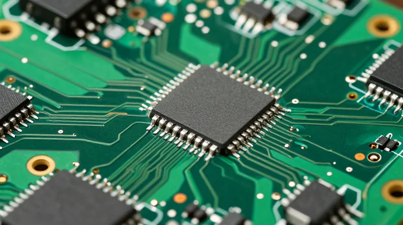
In the realm of advanced robotics, the controller is the central nervous system. As footprint requirements shrink and processing power intensifies, the transition from standard PCB fabrication to sub-millimeter precision is no longer optional—it is a functional requirement. Standard manufacturing tolerances, often calibrated for consumer electronics, introduce parasitic variances that can degrade high-speed signal integrity and lead to structural misalignments during complex PCBA assembly.
The Risks of Cumulative Tolerance Stacking
Cumulative errors occur when individual component placement deviations, pad geometry irregularities, and layer registration inaccuracies aggregate across a multi-stage assembly process. For precision robotic controllers, these errors are amplified by the extreme density of surface-mount devices (SMDs) and fine-pitch BGA interconnections.
| Parameter | Standard Tolerance | Precision Robotic Requirement |
|---|---|---|
| Registration Accuracy | ± 0.100 mm | ± 0.025 mm |
| Via Hole Diameter | ± 0.050 mm | ± 0.015 mm |
| Trace Width Variation | ± 20% | ± 5% |
Key Considerations for Designers
- Why do standard tolerances fail in robotics?
Standard tolerances allow for thermal expansion and signal jitter that can cause intermittent failures in high-vibration robotic environments, leading to unpredictable system behavior. - How does sub-millimeter precision improve PCBA reliability?
By minimizing pad-to-trace alignment errors, designers reduce the risk of solder bridging and cold joints, which are the primary failure points for controllers operating under constant mechanical stress. - What is the impact of layer registration?
In high-density interconnect (HDI) designs, even minor registration shifts can cause impedance discontinuities, directly affecting the timing accuracy of robotic sensory feedback loops.
Adhering to these stringent DFM rules necessitates an iterative design approach where CAD data is tightly coupled with the fabrication facility's real-time process capabilities. By enforcing tighter constraints early in the design cycle, engineers prevent the costly re-spins necessitated by assembly failure at the final integration phase.
Mastering Controlled Impedance in High-Density Interconnects

Strategies for Maintaining Signal Integrity
In robotic controllers where feedback loops operate in the gigahertz range, trace impedance deviations lead to signal reflections and jitter. To mitigate these, DFM protocols must prioritize the management of trace width etching, copper surface roughness, and the precise control of the prepreg-to-core dielectric constant (Dk) across the entire stack-up.
Critical Fabrication Parameters
| Parameter | Impact on Impedance | Recommended DFM Control |
|---|---|---|
| Trace Width | Inverse proportional change | Target +/- 5% tolerance |
| Dielectric Thickness | Directly impacts loop inductance | Verify resin content stability |
| Copper Roughness | High-frequency signal loss | Specify low-profile foil (VLP) |
Laminate Selection and Dielectric Management
For advanced robotic applications, choosing a laminate with a stable dielectric constant over a wide temperature range is mandatory. Fluctuations in ambient operating temperatures in industrial robotics can drift impedance values, potentially causing intermittent data corruption in encoders and real-time control buses.
Impedance Control FAQ
- How does etching tolerance impact differential pairs?
Improper etching causes width variations that skew differential impedance, leading to common-mode noise and increased EMI within the robotic controller. - Why is copper weight important for controlled impedance?
Heavier copper weights increase undercut risks during etching; using thinner foil (e.g., 0.5 oz) provides finer control over trace geometry and profile accuracy. - What role does fiber weave play in high-speed traces?
Glass-fiber weave patterns can cause localized impedance variations; choosing spread-glass fabrics or rotating designs at an angle helps normalize the signal path.
Advanced Thermal Management Strategies for Dense Assemblies
Advanced Thermal Management Strategies for Dense Assemblies
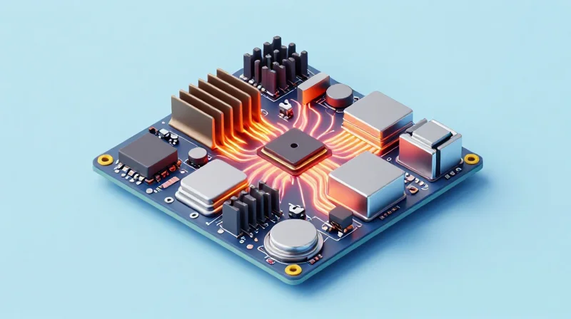
In precision robotic controllers, heat dissipation is not merely a component protection requirement but a critical factor in maintaining structural and electrical integrity. High-density designs often lead to localized hotspots that threaten solder joint reliability and induce impedance shifts. Designers must move beyond passive cooling by employing a holistic thermal strategy that utilizes the PCB itself as a primary heat-sink path.
Thermal Via Array Optimization
Thermal vias act as vertical conduits, transferring heat from power-dense components to internal copper planes or external heat sinks. For high-precision applications, the geometry and placement are paramount:
- Pitch and Density
Utilize a dense grid of 0.2mm to 0.3mm diameter vias directly under thermal pads, spaced at a 0.5mm pitch to balance thermal conductivity with structural PCB integrity. - Plating Thickness
Ensure via barrel plating thickness is consistent, ideally reaching 25um, to prevent thermal resistance bottlenecks within the board stackup. - Filling Techniques
For optimal efficiency, use copper-filled or conductive epoxy-filled vias to maximize the cross-sectional area of heat transfer, preventing solder wicking during assembly.
Material Selection and Comparative Performance
| Material Type | Thermal Conductivity (W/m-K) | Application Focus |
|---|---|---|
| Standard FR-4 | 0.25 - 0.35 | General logic control |
| High-Tg Thermally Conductive Laminate | 1.0 - 3.0 | Motor drivers and power stages |
| Metal Core (IMS/Aluminum) | 2.0 - 8.0 | Extreme high-current density |
Design Best Practices for Heat Path Integrity
To finalize the thermal design, ensure that high-power components are clustered to facilitate shared heat sinking without exceeding the maximum allowable junction temperature (Tj). Use large copper pours tied to internal ground planes via the thermal via arrays, ensuring these planes are not thermally isolated by high-speed signal routing.
Selecting the Optimal Surface Finish for Mission-Critical PCBA
For precision robotic controllers, surface finish selection transcends simple solderability; it must account for thermal cycling, mechanical stress, and potential chemical exposure. While standard finishes like HASL are often rejected due to uneven planarity, advanced alternatives offer the necessary characteristics for fine-pitch components, BGA packaging, and long-term storage requirements.
Comparative Analysis of Surface Finishes
| Finish | Reliability | Shelf Life | Wire Bondable |
|---|---|---|---|
| ENIG | High | Excellent | Yes |
| ENEPIG | Highest | Excellent | Yes |
| Immersion Silver | Moderate | Limited | No |
Technical Considerations for Robotic Applications
ENEPIG (Electroless Nickel Electroless Palladium Immersion Gold) has emerged as the gold standard for high-reliability robotic systems. By adding a palladium layer, it effectively eliminates the risk of 'black pad' syndrome associated with ENIG while providing an ultra-flat surface essential for miniature CSP and BGA components. Conversely, Immersion Silver provides a cost-effective alternative for high-speed signal integrity but requires stringent humidity controls during storage and assembly.
Surface Finish FAQs
- Why is ENEPIG preferred over ENIG for mission-critical controllers?
ENEPIG provides superior corrosion resistance and prevents nickel oxidation, ensuring long-term solder joint integrity under the high mechanical vibration typical of robotic environments. - Can Immersion Silver be used in long-term deployment environments?
Immersion Silver is susceptible to tarnish and creep corrosion in sulfur-rich environments, making it less suitable than gold-based finishes for mission-critical industrial hardware. - Does finish planarity impact assembly yield?
Yes. Non-planar finishes lead to uneven solder paste deposition, resulting in bridging or open circuits on fine-pitch pads, which is unacceptable for high-density robotic controller designs.
Precision Component Placement and SMT Optimization
Fiducial Strategy for Micro-Assembly
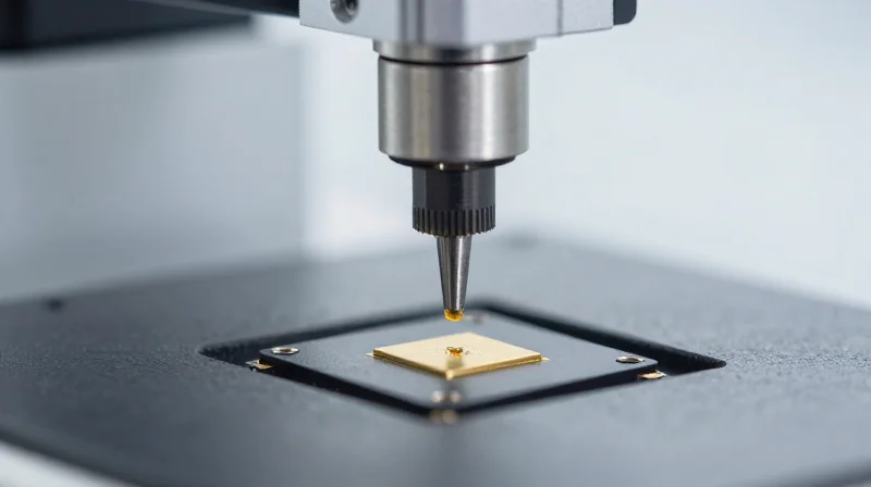
For robotic controllers utilizing 01005 components or fine-pitch BGA packages, standard board-level fiducials are insufficient. Precision assembly requires a hierarchical fiducial system. Global fiducials must be supplemented by local fiducials placed at opposite corners of fine-pitch footprints to compensate for potential substrate warp and local etching tolerances.
- What is the recommended size for local fiducials?
Local fiducials should be 0.5mm to 1.0mm in diameter, with a surrounding clearance zone at least twice the diameter, kept free of copper features to ensure consistent optical recognition. - Why are fiducial design constraints critical?
Improperly defined fiducials lead to misalignment in Pick-and-Place machines, causing solder bridging or tombstoning in miniaturized 01005 components.
Stencil Engineering and Paste Volume Control
Volume control is the primary driver of joint reliability in dense robotic controllers. Laser-cut stainless steel stencils with electropolished apertures are mandatory for 01005 geometries to minimize paste hang-up and ensure clean release.
| Component Type | Stencil Thickness | Aperture Design | Paste Requirement |
|---|---|---|---|
| 01005 | 0.08mm - 0.10mm | 1:1 or 0.9:1 (reduced) | Type 5 or 6 |
| 0.4mm BGA | 0.10mm - 0.12mm | Square/Rounded Square | Type 4 or 5 |
Advanced Optimization Workflow
def validate_dfm_clearance(component_size, clearance_mm):
    # Ensure minimum spacing for 01005 to prevent bridging
    min_clearance = 0.15 if component_size == '01005' else 0.25
    return clearance_mm >= min_clearance
Beyond stencil parameters, implementing vacuum-supported board fixtures during print cycles eliminates vibration-induced paste smearing. This synergy of software-guided fiducial recognition and physical support ensures that every solder deposit aligns perfectly with the pad, mitigating common failure modes in high-density robotic controller architectures.
The Role of Signal Integrity Analysis in Pre-Production

For precision robotic controllers, where high-speed signal integrity is non-negotiable, pre-production analysis acts as the final gatekeeper against failures. By performing electromagnetic (EM) field simulation before releasing files to fabrication, designers can identify impedance discontinuities, crosstalk, and potential EMI sources that traditional design rule checks (DRC) often miss. This shift-left approach reduces the reliance on costly physical prototypes and prevents late-stage design iterations that can severely impact project timelines.
Key Focus Areas in Signal Integrity Simulation
| Parameter | Risk Factor | Analysis Goal |
|---|---|---|
| Differential Pairs | Skew/Coupling Mismatch | Maintain tight phase alignment |
| Via Transitions | Impedance Discontinuity | Ensure consistent characteristic impedance |
| High-Speed Traces | Crosstalk/EM Emission | Verify isolation and return paths |
Essential DFM Integration Strategies
To effectively mitigate signal integrity issues, the following strategies should be hardcoded into the pre-production workflow for all robotic controller PCB assemblies:
- Field Solver Validation
Utilize 3D EM field solvers to verify stackup performance, specifically focusing on the dielectric constant (Dk) stability across the high-frequency range. - Return Path Continuity
Ensure that high-speed signals have a solid, uninterrupted reference plane to avoid parasitic inductance and radiation spikes. - Via Stubs Management
Perform back-drilling or minimize via stub lengths on high-speed transmission lines to eliminate signal reflections.
FAQs on Pre-Production Signal Integrity
- When is the optimal time to perform SI analysis?
Analysis should begin during the layout phase and reach completion before the final Gerber or ODB++ export, allowing for immediate design adjustments. - Does simulation guarantee hardware success?
Simulation significantly reduces risks, but it remains dependent on the accuracy of component models and material data provided to the solver.
Robust Verification and Testing Protocols
Integrated Testing Strategies for Robotic Control Systems
For precision robotic controllers, functional failure is not an option due to the potential for mechanical damage or catastrophic system downtime. A robust testing strategy integrates non-destructive inspections at every stage of the assembly process. By transitioning from sample-based quality checks to 100% automated inspection, manufacturers can achieve the high reliability required for motion control, sensor integration, and real-time processing circuitry.
| Testing Method | Primary Application | Detection Capability |
|---|---|---|
| AOI (Automated Optical Inspection) | Post-Reflow SMT | Missing, misaligned, or tombstoned components |
| AXI (Automated X-Ray Inspection) | BGA/QFN/LGA Assembly | Hidden solder voids, shorts, and bridging |
| Flying Probe Testing | Low to Mid-Volume PCBA | Open circuits, shorts, and component values |
Advanced Verification Workflow
The efficacy of these testing protocols relies on strict DFM integration. For instance, AXI requires that board designs account for copper pour avoidance beneath BGA footprints to prevent shadowing. Similarly, Flying Probe success is predicated on the availability of test points or accessible component leads, which must be defined during the layout phase. Establishing a closed-loop feedback mechanism ensures that inspection data informs real-time adjustments in stencil thickness or pick-and-place calibration, effectively mitigating recurring defects.
- Why is AXI mandatory for robotic controllers?
Robotic controllers frequently employ high-density ball grid arrays (BGA) and leadless packages. AXI is the only reliable method to visualize solder joint integrity beneath these components to detect internal micro-voids that lead to thermal fatigue. - How does Flying Probe complement AOI?
While AOI verifies the physical placement and polarity of components, Flying Probe validates the electrical connectivity of the netlist, ensuring that resistors, capacitors, and ICs meet specified values and that no unintended shorts exist within the internal PCB layers. - What role does DFM play in testing coverage?
DFM must prioritize 'Testability' by ensuring adequate clearance for probe contact and avoiding component overhangs that block optical or X-ray cameras, thereby maximizing the total coverage area during the automated inspection cycle.
Common DFM Pitfalls in Complex Robotic Hardware
Common DFM Pitfalls in Complex Robotic Hardware
Precision robotic controllers operate in high-vibration, high-EMI environments, making even minor DFM oversights catastrophic. Common failures often stem from inadequate thermal management, poor PCB stackup symmetry leading to board warpage, and improper component placement relative to mechanical constraints, which frequently cause solder joint fractures during field operations.
| Failure Mode | Common Cause | Impact on Robotics |
|---|---|---|
| Solder Joint Fatigue | Excessive board flex near connectors | Intermittent sensor data loss |
| Via-in-Pad Shorting | Inadequate plug/cap process | Internal shorts in multi-layer stacks |
| Thermal Throttling | Inadequate copper pours under FETs | Reduced motor control precision |
Critical DFM Checklist for Robotic Controllers
- Is thermal relief optimized?
Avoid complete thermal isolation for components handling high current; ensure adequate copper connectivity to prevent localized overheating while maintaining solderability. - Are high-mass components secured?
Heavy inductors or capacitors must be placed away from board-edge connectors where chassis-induced mechanical stress is highest. - Has stackup symmetry been verified?
Asymmetric copper distribution across layers often leads to board warpage during reflow, resulting in non-coplanar BGA solder joints. - Are fiducials sufficient?
Robotic assembly requires local fiducials near fine-pitch ICs to compensate for potential laminate shift during multi-stage reflow processes.
Designers must prioritize 'design for test' (DFT) alongside DFM. Implementing comprehensive test points and ensuring AOI (Automated Optical Inspection) accessibility are not optional luxuries but mandatory safeguards for maintaining high-yield production in sophisticated motion control systems.
Achieving sub-millimeter precision is not merely a design challenge; it is a manufacturing discipline. By integrating these advanced DFM practices early in your development cycle, you ensure that your robotic hardware remains robust, reliable, and performance-ready. Are you ready to optimize your next project for the factory floor? Contact our engineering team today to perform a comprehensive DFM review of your latest controller design.
