
In high-precision fields such as medical imaging and sensitive instrumentation, even the slightest magnetic signature can compromise system integrity. Designing for zero-magnetic interference is no longer an option but a necessity. This guide dives into the technical rigor required to achieve non-magnetic PCB excellence.
The Physics of Magnetic Interference in PCBs

The Physics of Magnetic Interference
In high-sensitivity environments, such as MRI machinery or quantum computing hardware, standard PCB materials act as significant sources of magnetic noise. The core issue lies in the magnetic permeability of metallic elements within the fabrication process, particularly nickel and iron alloys. Even trace amounts of ferromagnetic materials can distort local magnetic fields, creating deleterious induction currents and field inhomogeneity that compromise system precision.
Common Sources of Magnetic Signatures
- Electroless Nickel Immersion Gold (ENIG)
While popular for its planarity, the nickel layer is inherently ferromagnetic and must be strictly avoided in non-magnetic designs. - Ferrous Contamination
Manufacturing tools, such as drill bits and stainless steel transport fixtures, can leave microscopic ferrous particles embedded in the laminate substrate. - Component Lead Frames
Standard surface-mount components often utilize steel or Kovar leads, which exhibit significant magnetic susceptibility compared to copper or phosphor bronze.
Material Permeability Comparison
| Material | Magnetic Type | Suitability |
|---|---|---|
| Nickel | Ferromagnetic | Prohibited |
| Iron | Ferromagnetic | Prohibited |
| Copper | Diamagnetic | Ideal |
| Phosphor Bronze | Diamagnetic/Paramagnetic | High Suitability |
To mitigate these effects, designers must mandate fully non-magnetic plating processes, such as Immersion Silver (ImAg) or Electroless Nickel-Free Gold (ENEPIG using gold-only finishes). Furthermore, fabrication houses must implement rigorous cleanroom protocols to ensure that no ferrous residues from the drilling or routing process remain on the finished PCB, as these can accumulate over time and create unexpected magnetic signatures in the final assembly.
Stringent Material Vetting: Beyond Standard FR-4
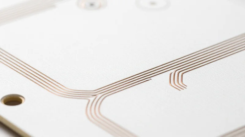
Achieving true non-magnetic performance in high-density interconnect (HDI) PCBs requires abandoning standard FR-4 and commodity materials, which often contain trace ferromagnetic contaminants within epoxy resin fillers or weave treatments. Engineers must prioritize specialized substrates characterized by low magnetic permeability and high structural stability to maintain signal integrity in environments where even minimal induction can compromise precision measurements.
Substrate Material Selection Criteria
The primary objective is the elimination of iron, nickel, or cobalt-based additives within the dielectric matrix. Standard glass fiber reinforcement must be replaced or verified for purity, as traditional sizing agents may introduce metallic precursors. High-frequency, low-loss materials such as PTFE-based composites or ceramic-filled laminates generally exhibit superior non-magnetic characteristics compared to standard epoxy-glass systems.
| Material Class | Magnetic Risk Profile | Suitability for Non-Magnetic HDI |
|---|---|---|
| Standard FR-4 | High (Contaminants) | Avoid |
| Ceramic-Filled Laminate | Low | Recommended |
| PTFE Composite | Very Low | Optimal |
| Polyimide (Non-Conductive) | Low | High-Temperature Use |
Metallurgical Vetting for Copper and Interconnects
Beyond the base substrate, the copper foil itself requires stringent scrutiny. Electrolytic copper foil must be certified free of magnetic impurities. Furthermore, common barrier platings—such as nickel, used in ENIG or ENEPIG finishes—are strictly prohibited in non-magnetic designs. Instead, engineers should specify immersion silver (ImAg) or immersion gold over electroless palladium (for specific applications) to prevent the introduction of ferromagnetic layers during the board finishing phase.
FAQs on Material Procurement
- Are all ceramic-filled laminates non-magnetic?
No. While they are superior to FR-4, you must request a Certificate of Conformance (CoC) confirming the absence of iron-based pigments or fillers in the ceramic compound. - How do I handle component attachment if nickel is forbidden?
Utilize direct solderable finishes or gold-plated surfaces and ensure that component leads and housings are verified as non-ferrous, typically by using copper or beryllium-copper alloy contacts. - Can standard prepreg be used in these designs?
Only if it is specifically identified as a 'non-magnetic grade' prepreg. Standard prepreg is a common source of iron-oxide contamination from manufacturing rollers.
Copper Purity Standards for Non-Magnetic Designs
The Imperative of Copper Purity in Magnetic Sensitivity
In the context of high-density PCB assemblies designed for sensitive instrumentation, standard commercial-grade copper foil is often insufficient due to trace impurities. Even infinitesimal concentrations of ferromagnetic elements—specifically iron, nickel, and cobalt—can create localized magnetic field distortions. For designs requiring near-zero magnetic permeability, sourcing Electro-Deposited (ED) or Rolled-Annealed (RA) copper with certified purity levels exceeding 99.99% is not merely a preference but a strict manufacturing requirement to maintain the integrity of the non-magnetic environment.
Common Contaminants and Their Magnetic Impact
| Element | Magnetic Property | Common Source | Impact |
|---|---|---|---|
| Iron (Fe) | Ferromagnetic | Raw ore / Refining equipment | High susceptibility to induction |
| Nickel (Ni) | Ferromagnetic | Plating baths / Additives | Significant magnetic noise |
| Cobalt (Co) | Ferromagnetic | Trace impurity in copper ore | Permanent magnetic interference |
Supply Chain Risks and Mitigation Strategies
Contamination often occurs during the copper refining process or via unintentional cross-contamination within the laminate manufacturing facility. Manufacturers must enforce a 'clean-line' protocol, ensuring that copper foils are processed on dedicated, isolated equipment to prevent contact with ferrous materials that might leave microscopic residues on the foil surface.
- How do trace amounts of iron affect high-frequency designs?
Iron creates localized variations in permeability, which can cause phase shifts and signal reflection in high-density, high-frequency circuits, effectively acting as an unwanted magnetic antenna. - Is electrolytic copper better than rolled copper for non-magnetic PCBs?
Electrolytic copper generally offers higher control over elemental purity during the electrolytic deposition process, whereas rolled copper may retain trace inclusions from the ingot casting phase if not strictly vetted. - What verification process should be used for incoming copper foil?
ICP-OES (Inductively Coupled Plasma Optical Emission Spectroscopy) analysis is the industry standard for quantifying trace metallic contaminants at the parts-per-million (PPM) level.
Optimizing Via Construction to Eliminate Eddy Currents
Minimizing Loop Area through Via Geometry
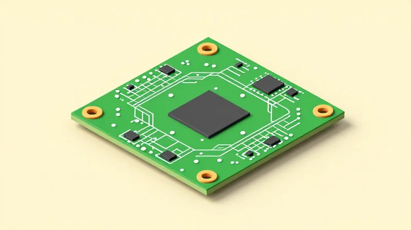
To mitigate eddy current formation in non-magnetic assemblies, the physical geometry of vias must be engineered to provide the shortest return path for high-frequency currents. In high-density designs, parasitic loops act as miniature antennas, which can be excited by stray fields. By employing back-drilling techniques to eliminate via stubs, designers can prevent resonant modes that contribute to unwanted inductive loops. Furthermore, keeping signal vias and their corresponding ground-return vias in close proximity—typically at the closest manufacturable spacing—is essential for canceling out magnetic field vectors.
Via Stitching and Shielding Strategies
Strategic via stitching acts as a Faraday cage for internal signal layers. By placing grounded vias along the perimeter of high-speed trace paths, designers constrain the electromagnetic field, effectively damping eddy currents that would otherwise circulate through the PCB substrate. When selecting plating processes for non-magnetic requirements, standard chemical copper deposition is preferred over processes that utilize nickel or cobalt-based additives, as these metals exhibit ferromagnetic properties even in trace amounts.
| Via Feature | Design Impact | Magnetic Risk Mitigation |
|---|---|---|
| Via Stubs | Increases return path length | Back-drill to eliminate resonant loops |
| Stitching Vias | Dampens electromagnetic field spread | Utilize dense ground via patterns |
| Plating Chemistry | Affects structural conductivity | Ensure non-magnetic copper-only deposition |
Frequently Asked Questions on Via Construction
- Does via-in-pad technology impact magnetic integrity?
Via-in-pad can improve performance by reducing path length, but ensure the fill material is non-conductive epoxy and the cap plating is purely copper to avoid introducing magnetic contaminants. - Why is electroless nickel immersion gold (ENIG) discouraged for these PCBs?
ENIG contains a nickel layer which is ferromagnetic; for strictly non-magnetic applications, specify Immersion Silver or Organic Solderability Preservative (OSP) instead. - How does via density affect eddy current suppression?
Higher via density allows for more precise return path management, which lowers the overall impedance and minimizes the loops where eddy currents can circulate.
Surface Finish Recommendations for Zero-Magnetic Performance
The Nickel Dilemma in Surface Finishes
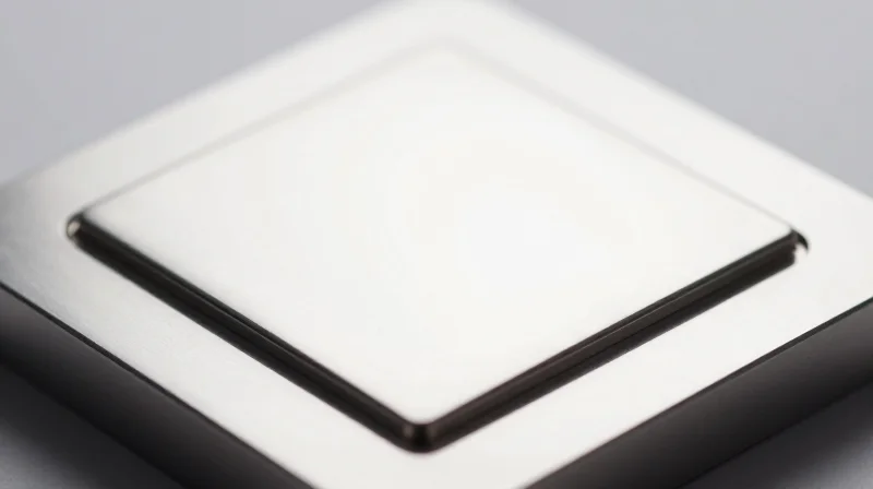
Standard industrial surface finishes often rely on electroless nickel as a diffusion barrier or conductive substrate. Because nickel is ferromagnetic, its presence creates a localized magnetic field that can compromise the performance of high-sensitivity non-magnetic assemblies. For designs requiring strict adherence to zero-magnetic performance, engineers must prioritize finishes that exclude nickel-bearing layers, such as ENIG or ENEPIG, in favor of direct-to-copper metallurgies.
Comparative Analysis of Non-Magnetic Finishes
| Finish Type | Nickel Content | Magnetic Risk | Best Application |
|---|---|---|---|
| ENIG | High | High | Standard non-critical |
| Immersion Silver | None | Low | High-density RF |
| Immersion Tin | None | Low | Cost-sensitive |
| OSP | None | None | Precision sensing |
Selecting the Optimal Finish
- Why is Immersion Silver preferred over ENIG?
Immersion Silver provides a conductive surface directly on copper without the need for a nickel barrier, eliminating the primary source of magnetism found in standard ENIG processes. - Does OSP offer advantages for non-magnetic boards?
Organic Solderability Preservatives (OSP) are inherently non-magnetic and provide a flat, copper-only interface, making them ideal for high-density interconnects where surface topography and magnetic neutrality are paramount. - Can I use hard gold for non-magnetic requirements?
Hard gold usually requires a nickel underlayer for durability. To use it in non-magnetic designs, you must explicitly specify a 'nickel-free' electrolytic gold process, which requires specialized handling to ensure proper adhesion to the copper base.
In addition to selecting the finish, process cleanliness is vital. Contamination from nickel-based polishing compounds or cross-contamination in automated plating lines can introduce trace ferromagnetic particulates that degrade the assembly's non-magnetic integrity. Always require certificate-of-conformance documentation from your fabricator to ensure the absence of electroless nickel in the final stack-up.
Critical Plating Techniques and Contamination Control
Mitigating Ferromagnetic Contamination in Plating Baths
In high-density non-magnetic PCB fabrication, the primary risk of magnetic contamination stems from particulate infiltration within electroless and electrolytic plating baths. Ferromagnetic ions—specifically Nickel (Ni) and Iron (Fe)—can leach into copper plating solutions if anodes are improperly maintained or if plating barrels have become degraded. Even trace metallic impurities, often introduced via recycled plating chemistry or contaminated additive chemistry, can aggregate during the high-aspect-ratio plating process, creating localized magnetic clusters that compromise signal integrity.
Comparison of Plating Risks
| Plating Process | Magnetic Risk Factor | Contamination Vector |
|---|---|---|
| Electroless Copper | High | Anode dissolution & bath aging |
| Electrolytic Copper | Moderate | Impure additives & porous baskets |
| Immersion Finishes | Low | Excessive dwell time (substrate leaching) |
Auditing the Manufacturing Line
To ensure non-magnetic performance, manufacturers must move beyond standard IPC inspections and implement a specialized audit protocol. The following best practices are essential for line validation in ultra-low-permeability applications.
- How is magnetic contamination detected in the bath?
Utilize Inductively Coupled Plasma Mass Spectrometry (ICP-MS) to monitor trace levels of Ni, Fe, and Co at the parts-per-billion (ppb) level, ensuring they remain below the susceptibility threshold. - What is the role of anode maintenance?
Use titanium anode baskets with fine-mesh auxiliary anode bags to prevent metallic particles from circulating in the plating solution and migrating into the high-density blind vias. - How do I verify the final assembly?
Perform periodic SQUID (Superconducting Quantum Interference Device) magnetometry on finished coupons to establish a baseline of magnetic permeability and identify processing-induced anomalies.
def validate_plating_chemistry(sample_data):
    thresholds = {'Ni': 0.05, 'Fe': 0.02, 'Co': 0.01} # ppm
    for metal, value in sample_data.items():
        if value > thresholds.get(metal, 0.1):
            raise ValueError(f'Contamination alert: {metal} exceeds safety limit')
    return True
DFM Checklist for Non-Magnetic Board Assembly
Checklist for Non-Magnetic PCB Assembly
Ensuring non-magnetic performance in high-density assemblies requires rigorous material selection, strictly controlled soldering environments, and validated inspection protocols to mitigate the risks of incidental ferromagnetic contamination.
- Component Verification
Audit all surface-mount and through-hole components using a high-sensitivity Gauss meter to confirm that leads, housings, and internal structures lack nickel or iron-based alloys. - Solder Alloy Selection
Utilize lead-free solders strictly formulated without nickel or cobalt additives; ensure batch certificates verify absence of magnetic impurities. - Tooling and Fixturing
Replace all standard steel-based assembly jigs, vacuum nozzles, and conveyor guides with non-magnetic alternatives such as aluminum, high-grade brass, or synthetic ceramics. - Contamination Prevention
Implement a dedicated cleanroom protocol to prevent the settling of airborne ferrous dust during solder paste printing and reflow processes.
Magnetic Interference Risk Matrix
| Source of Interference | Magnetic Risk Level | Mitigation Strategy |
|---|---|---|
| Nickel Underplating | Critical | Specify copper-only or chemical gold finishes. |
| Standard Steel Fixtures | High | Switch to ceramic or non-magnetic alloy tooling. |
| Ferrous Component Leads | High | Verify alloy composition via supplier audit. |
| Solder Contaminants | Medium | Strict batch testing and process cleanliness. |
Final Assembly Inspection Checklist
Before final shipment, apply these procedural checks to guarantee that no magnetic signature has been introduced during the assembly lifecycle.
- Post-Reflow Magnetometry
Perform a systematic magnetic field mapping across the entire board surface to detect local hot spots indicating residual contamination. - Automated Optical Inspection (AOI) Audit
Calibrate AOI systems to identify foreign object debris (FOD) that may have been introduced from machine environments. - Final Certification
Verify that all materials used in the assembly process, including flux and cleaning agents, have been certified as non-magnetic.
Testing and Verification: Validating Your Non-Magnetic Integrity

Quantitative Magnetic Signature Validation
Validating non-magnetic integrity requires moving beyond simple design compliance to rigorous empirical testing. Because standard manufacturing environments are prone to trace amounts of nickel or iron contamination, PCB fabricators must employ specialized instrumentation to quantify magnetic susceptibility. The primary objective is to verify that the board's magnetic permeability remains as close to vacuum permeability (μ₀) as possible, ensuring zero distortion in sensitive high-field environments.
| Testing Method | Applicability | Accuracy Level |
|---|---|---|
| Fluxgate Magnetometry | Board-level magnetic noise | High |
| Vibrating Sample Magnetometry (VSM) | Material samples/Plating integrity | Extreme |
| Hall Effect Scanning | Local field gradient mapping | Medium |
Standardized Verification Protocols
To maintain high-density non-magnetic performance, manufacturers must implement a multi-stage verification strategy that bridges the gap between raw material procurement and final assembly inspection.
- Baseline Characterization
Perform pre-production testing on substrate materials and copper foils to establish a magnetic baseline before chemical processing. - In-Process Contamination Audits
Conduct periodic ion-exchange monitoring and bath analysis to detect the introduction of ferromagnetic contaminants during electroless plating stages. - Final Assembly Field Mapping
Utilize a shielded cleanroom environment to map the magnetic signature of the fully populated PCB, confirming that component placement and soldering materials do not exceed allowable field constraints.
FAQ: Ensuring Non-Magnetic Compliance
- What is the acceptable threshold for magnetic permeability in these applications?
Typically, the relative permeability (μr) should be kept below 1.005. In extreme medical imaging applications, values approaching 1.000 are often mandated. - Can standard X-ray fluorescence (XRF) testing confirm non-magnetic integrity?
XRF is excellent for verifying the absence of nickel in finishes, but it cannot measure magnetic field distortions. It should be used as a supplementary quality check rather than the primary validation tool.
Achieving zero-magnetic signatures requires a holistic approach, from material selection to final assembly audits. By implementing these rigorous DFM rules, you ensure your technology meets the demands of the most sensitive environments. Contact our engineering team today to review your current designs for non-magnetic optimization.
